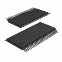
CBT6832CDGG,112 NXP Semiconductors, CBT6832CDGG,112 Datasheet - Page 5

CBT6832CDGG,112
Manufacturer Part Number
CBT6832CDGG,112
Description
IC 16BIT 1OF2 MUX/DEMUX 56TSSOP
Manufacturer
NXP Semiconductors
Series
74CBTr
Type
Multiplexer/Demultiplexerr
Datasheet
1.CBT6832CDGG112.pdf
(8 pages)
Specifications of CBT6832CDGG,112
Circuit
16 x 1:2
Independent Circuits
1
Current - Output High, Low
15mA, 64mA
Voltage Supply Source
Single Supply
Voltage - Supply
4.5 V ~ 5.5 V
Operating Temperature
0°C ~ 70°C
Mounting Type
Surface Mount
Package / Case
56-TSSOP
Lead Free Status / RoHS Status
Lead free / RoHS Compliant
Other names
935267058112
CBT6832CDG
CBT6832CDG
CBT6832CDG
CBT6832CDG
1. This parameter is warranted but not production tested. The propagation delay is based on the RC time constant of the typical on-state
Philips Semiconductors
AC CHARACTERISTICS
V
NOTES:
AC WAVEFORMS
V
2000 Jul 18
CC
M
Output Control
SYMBOL
SYMBOL
16-bit 1-of-2 multiplexer/demultiplexer with precharged outputs
and charge pump undershoot protection for live insertion
OUTPUT
Waveform 1. Input (An) to Output (Bn) Propagation Delays
resistance of the switch and a load capacitance of 50 pF, when driven by an ideal voltage source (zero output impedance).
Waveform 1
Waveform 2
= 1.5 V, V
INPUT
S1 at Open
(see Note)
(see Note)
t
t
t
t
t
t
= 5.0 V 0.5 V; GND = 0 V
(Low-level
PLH
PHL
PZH
PHZ
PZL
PLZ
Waveform 2. 3-State Output Enable and Disable Times
S1 at 7 V
enabling
Output
Output
Note:
Waveform 1 is for an output with internal conditions such that
the output is low except when disabled by the output control.
Waveform 2 is for an output with internal conditions such that
the output is high except when disabled by the output control.
t
PZH
IN
t
PZL
Propagation delay
A to B
Bus enable time
SEL to A, B
Bus disable time
SEL to A, B
= GND to 3.0 V
1.5V
t
PLH
1.5 V
1.5 V
1.2 V
1.5V
PARAMETER
PARAMETER
;
C
1
L
= 50 pF, R
t
PHZ
t
PLZ
1.5V
1.5 V
t
L
PHL
= 500
V
V
OL
OH
+ 0.3V
– 0.3V
1.5V
SA00530
SA00028
3V
0V
3.5V
V
V
0V
OL
OH
3 V
0 V
V
V
OH
OL
TEST CONDITIONS
TEST CONDITIONS
5
TEST CIRCUIT AND WAVEFORMS
DEFINITIONS
C
From Output
Under Test
L
=
C
Load capacitance includes jig and probe capacitance;
see AC CHARACTERISTICS for value.
L
= 50 pF
MIN
1
1
1
1
t
t
PHZ
PLZ
TEST
t
pd
/t
/t
PZL
PZH
500
Load Circuit
LIMITS
500
TYP
0.25
open
open
7 V
S1
S1
CBT6832C
Product specification
MAX
7.0
6.0
7.5
7.0
7 V
GND
SA00012
Open
UNIT
UNIT
ns
ns
ns


