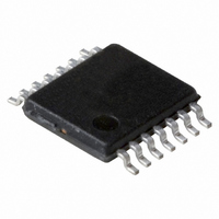
GTL2005PW,118 NXP Semiconductors, GTL2005PW,118 Datasheet - Page 11

GTL2005PW,118
Manufacturer Part Number
GTL2005PW,118
Description
IC XLATR QUAD BI-DIREC 14-TSSOP
Manufacturer
NXP Semiconductors
Datasheet
1.GTL2005PW118.pdf
(19 pages)
Specifications of GTL2005PW,118
Package / Case
14-TSSOP
Logic Function
Translator, Bidirectional
Number Of Bits
4
Input Type
GTL
Output Type
LVTTL, TTL
Number Of Channels
4
Number Of Outputs/channel
1
Differential - Input:output
No/No
Voltage - Supply
3 V ~ 3.6 V
Operating Temperature
-40°C ~ 85°C
Supply Voltage
3 V ~ 3.6 V
Logic Type
Translator
Logic Family
GTL
Translation
GTL/GTL+ to LVTTL/TTL
Input Bias Current (max)
3 mA
High Level Output Current
- 12 mA
Low Level Output Current
40 mA
Propagation Delay Time
4.4 ns (Typ) @ 3.3 V
Supply Voltage (max)
3.6 V
Supply Voltage (min)
3 V
Maximum Operating Temperature
+ 85 C
Minimum Operating Temperature
- 40 C
Mounting Style
SMD/SMT
Lead Free Status / RoHS Status
Lead free / RoHS Compliant
Data Rate
-
Lead Free Status / Rohs Status
Lead free / RoHS Compliant
Other names
568-1000-2
935263813118
GTL2005PW-T
935263813118
GTL2005PW-T
Available stocks
Company
Part Number
Manufacturer
Quantity
Price
Part Number:
GTL2005PW,118
Manufacturer:
NXP/恩智浦
Quantity:
20 000
NXP Semiconductors
11. Dynamic characteristics
Table 8.
V
[1]
GTL2005_7
Product data sheet
Symbol
GTL ; V
t
t
t
t
GTL; V
t
t
t
t
GTL+; V
t
t
t
t
PLH
PHL
PLH
PHL
PLH
PHL
PLH
PHL
PLH
PHL
PLH
PHL
CC
= 3.3 V
All typical values are at V
ref
ref
ref
= 0.8 V
= 0.6 V
= 1.0 V
Dynamic characteristics
0.3 V
Parameter
propagation delay, Bn to An
propagation delay, An to Bn
propagation delay, Bn to An
propagation delay, An to Bn
propagation delay, Bn to An
propagation delay, An to Bn
11.1 Waveforms
V
V
Fig 7.
M
M
CC
= 1.5 V at V
= V
= 3.3 V and T
a. Pulse duration
ref
V
Voltage waveforms
for A ports.
V
M
M
= 1.5 V for B port and V
amb
CC
t
p
= 25 C.
Quad GTL/GTL+ to LVTTL/TTL bidirectional non-latched translator
3.0 V; V
Rev. 07 — 3 February 2009
Conditions
see
see
see
see
see
see
V
M
Figure 7
Figure 8
Figure 7
Figure 8
Figure 7
Figure 8
M
002aab140
= V
ref
for A port
CC
/2 at V
3.0 V
0 V
CC
output
input
2.7 V for B ports and control pins;
Min
-
-
-
-
-
-
-
-
-
-
-
-
b. Propagation delay times
B port to A port
1.5 V
t
PLH
Typ
2.1
1.9
4.1
4.4
2.1
1.9
4.1
4.4
2.1
1.9
4.2
3.8
[1]
V
ref
Max
2.3
2.6
5.9
5.9
2.3
2.6
5.9
5.9
2.3
2.6
5.7
5.4
GTL2005
© NXP B.V. 2009. All rights reserved.
1.5 V
t
PHL
002aab141
V
Unit
ns
ns
ns
ns
ns
ns
ns
ns
ns
ns
ns
ns
ref
11 of 19
3.0 V
0 V
V
V
OH
OL


