74AVC1T45GW,125 NXP Semiconductors, 74AVC1T45GW,125 Datasheet
74AVC1T45GW,125
Specifications of 74AVC1T45GW,125
74AVC1T45GW-G
935284153125


Related parts for 74AVC1T45GW,125


74AVC1T45GW,125 Summary of contents
Page 1
Dual supply translating transceiver; 3-state Rev. 02 — 5 May 2009 1. General description The 74AVC1T45 is a single bit, dual supply transceiver with 3-state output that enables bidirectional level translation. It features one data input-output port (A and ...
Page 2
... NXP Semiconductors I Inputs accept voltages Low noise overshoot and undershoot < OFF I Multiple package options I Specified from +85 C and +125 C 3. Ordering information Table 1. Ordering information Type number Package Temperature range Name 74AVC1T45GW +125 C 74AVC1T45GM +125 C 4. Marking Table 2. Marking ...
Page 3
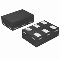
... NXP Semiconductors 6. Pinning information 6.1 Pinning 74AVC1T45 1 V CC(A) GND 001aag971 Fig 3. Pin configuration SOT363 6.2 Pin description Table 3. Pin description Symbol Pin V 1 CC(A) GND DIR CC(B) 7. Functional description [1] Table 4. Function table Supply voltage Input DIR CC(A) CC( ...
Page 4
... NXP Semiconductors 8. Limiting values Table 5. Limiting values In accordance with the Absolute Maximum Rating System (IEC 60134). Voltages are referenced to GND (ground = 0 V). Symbol Parameter V supply voltage port A CC(A) V supply voltage port B CC(B) I input clamping current IK V input voltage I I output clamping current ...
Page 5
... NXP Semiconductors 10. Static characteristics Table 7. Static characteristics At recommended operating conditions; voltages are referenced to GND (ground = 0 V). Symbol Parameter Conditions amb V HIGH-level V OH output voltage V LOW-level V OL output voltage I input leakage DIR input current V I OFF-state port output current V I power-off A port; V ...
Page 6
... NXP Semiconductors Table 7. Static characteristics At recommended operating conditions; voltages are referenced to GND (ground = 0 V). Symbol Parameter Conditions V HIGH-level V OH output voltage V LOW-level V OL output voltage I input leakage DIR input current V I OFF-state port output current V I power-off A port; V OFF leakage current V B port ...
Page 7
... NXP Semiconductors Table 7. Static characteristics At recommended operating conditions; voltages are referenced to GND (ground = 0 V). Symbol Parameter Conditions +125 C amb V HIGH-level data input IH input voltage DIR input V LOW-level data input IL input voltage DIR input V HIGH-level V OH output voltage V LOW-level V OL output voltage ...
Page 8
... NXP Semiconductors Table 7. Static characteristics At recommended operating conditions; voltages are referenced to GND (ground = 0 V). Symbol Parameter Conditions I power-off leakage A port; V OFF current V B port supply current A port port plus B port ( [ the supply voltage associated with the output port. CCO [ the supply voltage associated with the data input port. ...
Page 9
... NXP Semiconductors 11. Dynamic characteristics Table 8. Typical dynamic characteristics at V Voltages are referenced to GND (ground = 0 V); for test circuit see Symbol Parameter Conditions t propagation delay disable time DIR to A dis DIR enable time DIR DIR the same as t and PLH PHL ...
Page 10
... NXP Semiconductors Table 11. Dynamic characteristics for temperature range +85 C Voltages are referenced to GND (ground = 0 V); for test circuit see Symbol Parameter Conditions 1.3 V CC(A) t propagation delay disable time DIR to A dis DIR enable time DIR DIR 1 1.6 V CC(A) t propagation delay ...
Page 11
... NXP Semiconductors Table 12. Dynamic characteristics for temperature range +125 C Voltages are referenced to GND (ground = 0 V); for test circuit see Symbol Parameter Conditions 1.3 V CC(A) t propagation delay disable time DIR to A dis DIR enable time DIR DIR 1 1.6 V CC(A) t propagation delay ...
Page 12
... NXP Semiconductors 12. Waveforms Measurement points are given in V and V are typical output voltage drops that occur with the output load Fig 5. The data input ( output (B, A) propagation delay times DIR input output LOW-to-OFF OFF-to-LOW output HIGH-to-OFF OFF-to-HIGH Measurement points are given in ...
Page 13
... NXP Semiconductors Test data is given in Table R = Load resistance Load capacitance including jig and probe capacitance Termination resistance External voltage for measuring switching times. EXT Fig 7. Load circuitry for switching times Table 14. Test data Supply voltage Input [ CC(A) CC( CCI 1. 2.7 V ...
Page 14
... NXP Semiconductors 13. Application information 13.1 Unidirectional logic level-shifting application The circuit given in unidirectional logic level-shifting application. Fig 8. Table 15. Pin 74AVC1T45_2 Product data sheet Figure example of the 74AVC1T45 being used CC1 V CC(A) 1 GND V CC1 system-1 Unidirectional logic level-shifting application Description unidirectional logic level-shifting application ...
Page 15
... NXP Semiconductors 13.2 Bidirectional logic level-shifting application Figure 9 application. Since the device does not have an output enable pin, the system designer should take precautions to avoid bus contention between system-1 and system-2 when changing directions. V I/O-1 DIR CTRL Fig 9. Table 16 and then from system-2 to system-1. ...
Page 16
... NXP Semiconductors 13.3 Power-up considerations The device is designed such that no special power-up sequence is required other than GND being applied first. Table 17. V CC( 0.8 V 1.2 V 1.5 V 1.8 V 2.5 V 3.3 V 13.4 Enable times Calculate the enable times for the 74AVC1T45 using the following formulas: • ...
Page 17
... NXP Semiconductors 14. Package outline Plastic surface-mounted package; 6 leads y 6 pin 1 index DIMENSIONS (mm are the original dimensions UNIT max 0.30 1.1 0.25 mm 0.1 0.20 0.10 0.8 OUTLINE VERSION IEC SOT363 Fig 10. Package outline SOT363 (SC-88) 74AVC1T45_2 Product data sheet scale 2.2 1.35 2 ...
Page 18
... NXP Semiconductors XSON6: plastic extremely thin small outline package; no leads; 6 terminals; body 1 x 1. (2) terminal 1 index area DIMENSIONS (mm are the original dimensions) ( UNIT b D max max 0.25 1.5 mm 0.5 0.04 0.17 1.4 Notes 1. Including plating thickness. 2. Can be visible in some manufacturing processes. ...
Page 19
... NXP Semiconductors 15. Abbreviations Table 18. Abbreviations Acronym Description CDM Charged Device Model CMOS Complementary Metal Oxide Semiconductor DUT Device Under Test ESD ElectroStatic Discharge HBM Human Body Model MM Machine Model 16. Revision history Table 19. Revision history Document ID Release date 74AVC1T45_2 20090505 • Modifications: ...
Page 20
... Right to make changes — NXP Semiconductors reserves the right to make changes to information published in this document, including without limitation specifications and product descriptions, at any time and without notice ...
Page 21
... NXP Semiconductors 19. Contents 1 General description . . . . . . . . . . . . . . . . . . . . . . 1 2 Features . . . . . . . . . . . . . . . . . . . . . . . . . . . . . . . 1 3 Ordering information . . . . . . . . . . . . . . . . . . . . . 2 4 Marking . . . . . . . . . . . . . . . . . . . . . . . . . . . . . . . . 2 5 Functional diagram . . . . . . . . . . . . . . . . . . . . . . 2 6 Pinning information . . . . . . . . . . . . . . . . . . . . . . 3 6.1 Pinning . . . . . . . . . . . . . . . . . . . . . . . . . . . . . . . 3 6.2 Pin description . . . . . . . . . . . . . . . . . . . . . . . . . 3 7 Functional description . . . . . . . . . . . . . . . . . . . 3 8 Limiting values Recommended operating conditions Static characteristics Dynamic characteristics . . . . . . . . . . . . . . . . . . 9 12 Waveforms . . . . . . . . . . . . . . . . . . . . . . . . . . . . 12 13 Application information ...