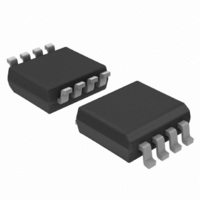
74AVC2T45DC,125 NXP Semiconductors, 74AVC2T45DC,125 Datasheet - Page 11

74AVC2T45DC,125
Manufacturer Part Number
74AVC2T45DC,125
Description
IC BUS TRANSCVR TRI-ST DL 8VSSOP
Manufacturer
NXP Semiconductors
Series
74AVCr
Datasheet
1.74AVC2T45GT115.pdf
(27 pages)
Specifications of 74AVC2T45DC,125
Package / Case
US8, 8-VSSOP
Logic Function
Translator, Bidirectional, 3-State
Number Of Bits
2
Input Type
Logic
Output Type
Logic
Number Of Channels
2
Number Of Outputs/channel
1
Differential - Input:output
No/No
Propagation Delay (max)
2.4ns
Voltage - Supply
0.8 V ~ 3.6 V
Operating Temperature
-40°C ~ 125°C
Supply Voltage
0.8 V ~ 3.6 V
Mounting Style
SMD/SMT
Lead Free Status / RoHS Status
Lead free / RoHS Compliant
Data Rate
-
Lead Free Status / Rohs Status
Lead free / RoHS Compliant
Other names
74AVC2T45DC-G
74AVC2T45DC-G
935283716125
74AVC2T45DC-G
935283716125
Available stocks
Company
Part Number
Manufacturer
Quantity
Price
Part Number:
74AVC2T45DC,125
Manufacturer:
NXP/恩智浦
Quantity:
20 000
NXP Semiconductors
Table 13.
Voltages are referenced to GND (ground = 0 V); for test circuit see
[1]
74AVC2T45
Product data sheet
Symbol Parameter
V
t
t
t
V
t
t
t
V
t
t
t
V
t
t
t
V
t
t
t
pd
dis
en
pd
dis
en
pd
dis
en
pd
dis
en
pd
dis
en
CC(A)
CC(A)
CC(A)
CC(A)
CC(A)
t
t
pd
en
is the same as t
is a calculated value using the formula shown in
= 1.1 V to 1.3 V
= 1.4 V to 1.6 V
= 1.65 V to 1.95 V
= 2.3 V to 2.7 V
= 3.0 V to 3.6 V
propagation
delay
disable time
enable time
propagation
delay
disable time
enable time
propagation
delay
disable time
enable time
propagation
delay
disable time
enable time
propagation
delay
disable time
enable time
Dynamic characteristics for temperature range −40 °C to +125 °C
PLH
and t
Conditions
A to B
B to A
DIR to A
DIR to B
DIR to A
DIR to B
A to B
B to A
DIR to A
DIR to B
DIR to A
DIR to B
A to B
B to A
DIR to A
DIR to B
DIR to A
DIR to B
A to B
B to A
DIR to A
DIR to B
DIR to A
DIR to B
A to B
B to A
DIR to A
DIR to B
DIR to A
DIR to B
PHL
; t
dis
is the same as t
V
1.2 V ± 0.1 V
Min
CC(B)
1.0
1.0
2.2
1.0
1.0
2.0
1.0
1.0
1.8
1.0
1.0
1.7
1.0
1.0
1.7
2.2
1.6
1.6
1.5
1.5
-
-
-
-
-
-
-
-
-
-
All information provided in this document is subject to legal disclaimers.
Dual-bit, dual-supply voltage level translator/transceiver; 3-state
Max
19.1
19.6
15.8
15.8
15.3
14.6
14.3
12.7
14.7
13.1
9.9
9.9
9.2
8.8
7.5
8.3
8.5
6.8
8.5
8.0
6.3
8.0
7.9
6.8
7.9
Rev. 5 — 30 November 2010
9.7
7.0
6.1
4.7
5.2
Section 13.4 “Enable times”
PLZ
and t
1.5 V ± 0.1 V 1.8 V ± 0.15 V 2.5 V ± 0.2 V
Min
0.7
0.8
1.8
0.7
0.8
1.8
0.6
0.7
1.8
0.5
0.6
2.0
0.5
0.6
0.7
2.2
1.6
1.6
1.5
1.5
-
-
-
-
-
-
-
-
-
-
PHZ
; t
en
Max
16.2
17.2
12.5
13.0
11.4
11.8
10.0
10.1
10.2
7.5
8.8
9.7
7.4
6.0
6.0
7.0
6.5
5.7
5.1
6.1
6.3
5.2
4.2
4.7
5.8
9.9
5.0
4.0
5.2
6.1
is the same as t
Figure
Min
0.6
0.7
2.2
2.0
0.6
0.7
1.6
1.6
0.5
0.5
1.6
1.4
0.5
0.5
1.5
1.5
0.5
0.5
1.5
0.6
8; for wave forms see
-
-
-
-
-
-
-
-
-
-
PZL
Max
16.1
16.5
12.3
12.1
10.9
11.3
6.8
8.5
9.7
7.6
5.1
5.7
7.0
6.6
4.8
4.9
6.1
6.4
4.3
3.8
4.7
5.7
9.5
9.0
4.1
3.5
5.2
6.1
9.6
9.3
[1]
and t
PZH
Min
0.5
0.6
2.2
1.7
0.5
0.6
1.6
1.2
0.5
0.5
1.6
1.0
0.5
0.5
1.5
0.6
0.5
0.5
1.5
0.7
-
-
-
-
-
-
-
-
-
-
.
Max
14.9
16.0
10.5
Figure 6
11.1
6.3
8.0
9.7
6.9
4.1
5.2
7.0
5.3
3.8
4.3
6.1
5.0
9.3
9.9
3.3
3.3
4.7
4.7
8.0
8.0
3.1
2.9
5.2
4.6
7.5
8.3
74AVC2T45
3.3 V ± 0.3 V
© NXP B.V. 2010. All rights reserved.
Min
0.5
0.5
2.2
2.4
0.5
0.5
1.6
1.7
0.5
0.5
1.6
1.5
0.5
0.5
1.5
1.1
0.5
0.5
1.5
1.7
and
-
-
-
-
-
-
-
-
-
-
Figure 7
Max
15.9
16.5
10.9
11.1
6.8
7.9
9.7
8.0
3.9
5.0
7.0
6.1
3.5
4.1
6.1
5.8
9.9
9.6
2.9
3.1
4.7
5.3
8.4
7.6
2.7
2.7
5.2
5.2
7.9
7.9
11 of 27
Unit
ns
ns
ns
ns
ns
ns
ns
ns
ns
ns
ns
ns
ns
ns
ns
ns
ns
ns
ns
ns
ns
ns
ns
ns
ns
ns
ns
ns
ns
ns


