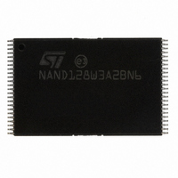
NAND128W3A2BN6E NUMONYX, NAND128W3A2BN6E Datasheet - Page 16

NAND128W3A2BN6E
Manufacturer Part Number
NAND128W3A2BN6E
Description
IC FLASH 128MBIT 48TSOP
Manufacturer
NUMONYX
Specifications of NAND128W3A2BN6E
Format - Memory
FLASH
Memory Type
FLASH - Nand
Memory Size
128M (16M x 8)
Interface
Parallel
Voltage - Supply
2.7 V ~ 3.6 V
Operating Temperature
-40°C ~ 85°C
Package / Case
48-TSOP
Access Time
12µs
Supply Voltage Range
2.7V To 3.6V
Memory Case Style
TSOP
No. Of Pins
48
Operating Temperature Range
-40°C To +85°C
Voltage, Vcc
3.3V
Rohs Compliant
Yes
Lead Free Status / RoHS Status
Lead free / RoHS Compliant
Speed
-
Lead Free Status / RoHS Status
Lead free / RoHS Compliant, Lead free / RoHS Compliant
Other names
497-5037
497-5037
497-5037
Available stocks
Company
Part Number
Manufacturer
Quantity
Price
Company:
Part Number:
NAND128W3A2BN6E
Manufacturer:
MICRON
Quantity:
3 000
Part Number:
NAND128W3A2BN6E
Manufacturer:
ST
Quantity:
20 000
Signal descriptions
3
3.1
3.2
3.3
3.4
3.5
16/59
Signal descriptions
See
connected to this device.
Inputs/outputs (I/O0-I/O7)
Input/outputs 0 to 7 input the selected address, output the data during a read operation or
input a command or data during a write operation. The inputs are latched on the rising edge
of Write Enable. I/O0-I/O7 are left floating when the device is deselected or the outputs are
disabled.
Inputs/outputs (I/O8-I/O15)
Input/outputs 8 to 15 are only available in x16 devices. They output the data during a read
operation or input data during a write operation. Command and address inputs only require
I/O0 to I/O7.
The inputs are latched on the rising edge of Write Enable. I/O8-I/O15 are left floating when
the device is deselected or the outputs are disabled.
Address Latch Enable (AL)
Address Latch Enable activates the latching of the address inputs in the command interface.
When AL is high, the inputs are latched on the rising edge of Write Enable.
Command Latch Enable (CL)
The Command Latch Enable activates the latching of the command inputs in the command
interface. When CL is high, the inputs are latched on the rising edge of Write Enable.
Chip Enable (E)
The Chip Enable input activates the memory control logic, input buffers, decoders and
sense amplifiers. When Chip Enable is Low, V
While the device is busy programming or erasing, Chip Enable transitions to High (V
ignored and the device does not go into standby mode.
While the device is busy reading:
Figure 1: Logic diagram
the Chip Enable input should be held Low during the whole busy time (t
devices that do not feature the Chip Enable don’t care option. Otherwise, the read
operation in progress is interrupted and the device goes into standby mode.
for devices that feature the Chip Enable don’t care option, the Chip Enable going High
during the busy time (t
go into standby mode.
BLBH1
and
) will not interrupt the read operation and the device will not
Table 3: Signal names
IL
, the device is selected.
for a brief overview of the signals
NAND128-A, NAND256-A
BLBH1
) for
IH
) are


