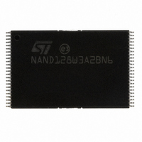
NAND128W3A2BN6E NUMONYX, NAND128W3A2BN6E Datasheet - Page 30

NAND128W3A2BN6E
Manufacturer Part Number
NAND128W3A2BN6E
Description
IC FLASH 128MBIT 48TSOP
Manufacturer
NUMONYX
Specifications of NAND128W3A2BN6E
Format - Memory
FLASH
Memory Type
FLASH - Nand
Memory Size
128M (16M x 8)
Interface
Parallel
Voltage - Supply
2.7 V ~ 3.6 V
Operating Temperature
-40°C ~ 85°C
Package / Case
48-TSOP
Access Time
12µs
Supply Voltage Range
2.7V To 3.6V
Memory Case Style
TSOP
No. Of Pins
48
Operating Temperature Range
-40°C To +85°C
Voltage, Vcc
3.3V
Rohs Compliant
Yes
Lead Free Status / RoHS Status
Lead free / RoHS Compliant
Speed
-
Lead Free Status / RoHS Status
Lead free / RoHS Compliant, Lead free / RoHS Compliant
Other names
497-5037
497-5037
497-5037
Available stocks
Company
Part Number
Manufacturer
Quantity
Price
Company:
Part Number:
NAND128W3A2BN6E
Manufacturer:
MICRON
Quantity:
3 000
Part Number:
NAND128W3A2BN6E
Manufacturer:
ST
Quantity:
20 000
Device operations
6.7.1
6.7.2
6.7.3
6.8
30/59
After the read status register command has been issued, the device remains in read status
register mode until another command is issued. therefore if a read status register command
is issued during a random read cycle a new read command must be issued to continue with
a page read.
The status register bits are summarized in
refer in conjunction with the following sections.
Write protection bit (SR7)
The write protection bit identifies if the device is protected or not. If the write protection bit is
set to ‘1’ the device is not protected and program or erase operations are allowed. If the
write protection bit is set to ‘0’ the device is protected and program or erase operations are
not allowed.
P/E/R controller bit (SR6)
The program/erase/read controller bit indicates whether the P/E/R controller is active or
inactive. When the P/E/R controller bit is set to ‘0’, the P/E/R controller is active (device is
busy); when the bit is set to ‘1’, the P/E/R controller is inactive (device is ready).
Error bit (SR0)
The error bit identifies if any errors have been detected by the P/E/R controller. The error bit
is set to ’1’ when a program or erase operation has failed to write the correct data to the
memory. If the error bit is set to ‘0’ the operation has completed successfully.
SR5, SR4, SR3, SR2 and SR1 are reserved.
Table 11.
Read electronic signature
The device contains a manufacturer code and device code. To read these codes the following
two steps are required:
1.
2.
SR5, SR4, SR3,
SR2, SR1
First use one bus write cycle to issue the Read Electronic Signature command (90h),
followed by an address input of 00h.
Then, perform two bus read operations. The first one reads the manufacturer code and
the second reads the device code. Further bus read operations are ignored.
SR7
SR6
SR0
Bit
Status register bits
Program/erase/read
Write protection
Generic error
Reserved
controller
Name
Table 11: Status register
Logic level
’don’t care’
'1'
'0'
'1'
'0'
‘1’
‘0’
Not protected
Protected
P/E/R C inactive, device ready
P/E/R C active, device busy
Error – operation failed
No error – operation successful
NAND128-A, NAND256-A
bits, to which you should
Definition


