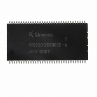
HYB25D128800CE-6 Qimonda, HYB25D128800CE-6 Datasheet - Page 28

HYB25D128800CE-6
Manufacturer Part Number
HYB25D128800CE-6
Description
IC DDR SDRAM 128MBIT 66TSOP
Manufacturer
Qimonda
Datasheet
1.HYB25D128800CE-6.pdf
(35 pages)
Specifications of HYB25D128800CE-6
Format - Memory
RAM
Memory Type
DDR SDRAM
Memory Size
128M (16M x 8)
Speed
166MHz
Interface
Parallel
Voltage - Supply
2.3 V ~ 2.7 V
Operating Temperature
0°C ~ 70°C
Package / Case
66-TSOPII
Lead Free Status / RoHS Status
Lead free / RoHS Compliant
Other names
675-1005-2
Available stocks
Company
Part Number
Manufacturer
Quantity
Price
Company:
Part Number:
HYB25D128800CE-6
Manufacturer:
INFENION
Quantity:
417
11) The specific requirement is that DQS be valid (HIGH, LOW, or some point on a valid transition) on or before this CK edge. A valid transition
12) The maximum limit for this parameter is not a device limit. The device operates with a greater value for this parameter, but system
Rev. 1.51, 2006-09
03292006-U5AN-6TI1
Parameter
DQ output access time from CK/CK
CK high-level width
Clock cycle time
CK low-level width
Auto precharge write recovery + precharge time
DQ and DM input hold time
DQ and DM input pulse width (each input)
DQS output access time from CK/CK
DQS input low (high) pulse width (write cycle)
DQS-DQ skew (DQS and associated DQ signals)
DQS-DQ skew (DQS and associated DQ signals)
Write command to 1
DQ and DM input setup time
DQS falling edge hold time from CK (write cycle)
DQS falling edge to CK setup time (write cycle)
Clock Half Period
Data-out high-impedance time from CK/CK
Address and control input hold time
Control and Addr. input pulse width (each input)
Address and control input setup time
Data-out low-impedance time from CK/CK
Mode register set command cycle time
DQ/DQS output hold time
is defined as monotonic and meeting the input slew rate specifications of the device. When no writes were previously in progress on the
bus, DQS will be transitioning from Hi-Z to logic LOW. If a previous write was in progress, DQS could be HIGH, LOW, or transitioning from
HIGH to LOW at this time, depending on
performance (bus turnaround) degrades accordingly.
st
DQS latching transition
t
DQSS
.
28
Symbol
t
t
t
t
t
t
t
t
t
t
t
t
t
t
t
t
t
t
t
t
t
t
t
AC
CH
CK
CL
DAL
DH
DIPW
DQSCK
DQSL,H
DQSQ
DQSQ
DQSS
DS
DSH
DSS
HP
HZ
IH
IPW
IS
LZ
MRD
QH
–7
DDR266A
Min.
–0.75
0.45
7.5
7.5
7.5
0.45
(
0.5
1.75
–0.75
0.35
—
—
0.75
0.5
0.2
0.2
min. (
—
0.9
1.0
2.2
0.9
1.0
–0.75
2
t
HP
AC Timing - Absolute Specifications for
t
WR
–
/
t
t
CK
QHS
t
CL
)+(
,
t
t
CH
RP
128-Mbit Double-Data-Rate SDRAM
)
/
t
CK
)
Max.
+0.75
0.55
12
12
12
0.55
—
—
+0.75
—
+0.5
+0.5
1.25
—
—
—
—
+0.75
—
1.1
—
—
—
+0.75
—
—
HYB25D128xxxC[C/E/F/T](L)
Unit Note
ns
t
ns
ns
ns
t
t
ns
ns
ns
t
ns
ns
t
ns
t
t
ns
ns
ns
ns
ns
ns
ns
ns
t
ns
CK
CK
CK
CK
CK
CK
CK
CK
Internet Data Sheet
Condition
2)3)4)5)
CL = 3.0
CL = 2.5
CL = 2.0
6)
TFBGA
TSOPII
7)
fast slew rate
8)
slow slew rate
9)
fast slew rate
slow slew rate
TABLE 23
1)
/ Test
–7


