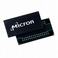
MT47H32M8BP-37E:B TR Micron Technology Inc, MT47H32M8BP-37E:B TR Datasheet - Page 92

MT47H32M8BP-37E:B TR
Manufacturer Part Number
MT47H32M8BP-37E:B TR
Description
IC DDR2 SDRAM 256MBIT 60FBGA
Manufacturer
Micron Technology Inc
Type
DDR2 SDRAMr
Datasheet
1.MT47H16M16BG-3B_TR.pdf
(128 pages)
Specifications of MT47H32M8BP-37E:B TR
Format - Memory
RAM
Memory Type
DDR2 SDRAM
Memory Size
256M (32M x 8)
Speed
3.75ns
Interface
Parallel
Voltage - Supply
1.7 V ~ 1.9 V
Operating Temperature
0°C ~ 85°C
Package / Case
60-FBGA
Organization
32Mx8
Density
256Mb
Address Bus
15b
Access Time (max)
500ps
Maximum Clock Rate
533MHz
Operating Supply Voltage (typ)
1.8V
Package Type
FBGA
Operating Temp Range
0C to 85C
Operating Supply Voltage (max)
1.9V
Operating Supply Voltage (min)
1.7V
Supply Current
160mA
Pin Count
60
Mounting
Surface Mount
Operating Temperature Classification
Commercial
Lead Free Status / RoHS Status
Lead free / RoHS Compliant
Other names
557-1049-2
- Current page: 92 of 128
- Download datasheet (10Mb)
Figure 49: READ-to-PRECHARGE – BL = 4
Figure 50: READ-to-PRECHARGE – BL = 8
PDF: 09005aef8117c187
256MbDDR2.pdf - Rev. M 7/09 EN
Notes:
Notes:
not be issued until
the access of the last data elements.
Examples of READ-to-PRECHARGE for BL = 4 are shown in Figure 49 and in Figure 50
for BL = 8. The delay from READ-to-PRECHARGE period to the same bank is AL + BL/
2 - 2CK + MAX (
DQS, DQS#
DQS, DQS#
Command
Command
Address
Address
1. RL = 4 (AL = 1, CL = 3); BL = 4.
2.
3. Shown with nominal
1. RL = 4 (AL = 1, CL = 3); BL = 8.
2.
3. Shown with nominal
CK#
A10
DQ
CK#
A10
CK
DQ
CK
t
t
RTP ≥ 2 clocks.
RTP ≥ 2 clocks.
Bank a
Bank a
READ
READ
T0
T0
AL + BL/2 - 2CK + MAX ( t RTP/ t CK or 2CK)
AL = 1
AL = 1
First 4-bit
t
prefetch
RTP/
prefetch
NOP
AL + BL/2 - 2CK + MAX ( t RTP/ t CK or 2CK)
4-bit
T1
≥ t RAS (MIN)
NOP
T1
t
RP is met. However, part of the row precharge time is hidden during
t
CK or 2 × CK) where MAX means the larger of the two.
≥t RAS (MIN)
≥ t RTP (MIN)
NOP
T2
t
t
AC,
AC,
NOP
CL = 3
T2
Second 4-bit
92
t
t
DQSCK, and
DQSCK, and
CL = 3
prefetch
≥ t RC (MIN)
≥t RC (MIN)
NOP
T3
Bank a
Valid
PRE
T3
≥t RTP (MIN)
Micron Technology, Inc. reserves the right to change products or specifications without notice.
NOP
T4
t
DO
t
DQSQ.
DQSQ.
256Mb: x4, x8, x16 DDR2 SDRAM
NOP
T4
≥ t RP (MIN)
DO
DO
Bank a
Valid
PRE
T5
DO
DO
NOP
T5
Transitioning Data
Transitioning Data
DO
DO
NOP
T6
≥t RP (MIN)
DO
DO
Bank a
Valid
ACT
T6
DO
©2003 Micron Technology, Inc. All rights reserved.
NOP
T7
DO
Don’t Care
Don’t Care
DO
NOP
T7
Bank a
Valid
ACT
T8
READ
Related parts for MT47H32M8BP-37E:B TR
Image
Part Number
Description
Manufacturer
Datasheet
Request
R

Part Number:
Description:
IC DDR2 SDRAM 256MBIT 5NS 60FBGA
Manufacturer:
Micron Technology Inc
Datasheet:

Part Number:
Description:
Manufacturer:
Micron Technology Inc
Datasheet:

Part Number:
Description:
IC DDR2 SDRAM 256MB 60-FBGA
Manufacturer:
Micron Technology Inc
Datasheet:

Part Number:
Description:
IC DDR2 SDRAM 256MBIT 5NS 60FBGA
Manufacturer:
Micron Technology Inc
Datasheet:

Part Number:
Description:
IC DDR2 SDRAM 256MBIT 60FBGA
Manufacturer:
Micron Technology Inc
Datasheet:

Part Number:
Description:
Manufacturer:
Micron Technology Inc
Datasheet:

Part Number:
Description:
Manufacturer:
Micron Technology Inc
Datasheet:

Part Number:
Description:
Manufacturer:
Micron Technology Inc
Datasheet:

Part Number:
Description:
Manufacturer:
Micron Technology Inc
Datasheet:

Part Number:
Description:
IC SDRAM 64MBIT 133MHZ 54TSOP
Manufacturer:
Micron Technology Inc
Datasheet:

Part Number:
Description:
IC SDRAM 64MBIT 5.5NS 86TSOP
Manufacturer:
Micron Technology Inc
Datasheet:

Part Number:
Description:
IC SDRAM 64MBIT 200MHZ 86TSOP
Manufacturer:
Micron Technology Inc
Datasheet:

Part Number:
Description:
IC SDRAM 64MBIT 133MHZ 54TSOP
Manufacturer:
Micron Technology Inc
Datasheet:

Part Number:
Description:
IC SDRAM 128MBIT 133MHZ 54TSOP
Manufacturer:
Micron Technology Inc
Datasheet:

Part Number:
Description:
IC SDRAM 256MBIT 133MHZ 90VFBGA
Manufacturer:
Micron Technology Inc
Datasheet:


