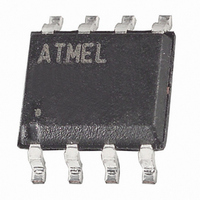
AT45DB021D-SH-T Atmel, AT45DB021D-SH-T Datasheet - Page 5

AT45DB021D-SH-T
Manufacturer Part Number
AT45DB021D-SH-T
Description
IC FLASH 2MBIT 66MHZ 8SOIC
Manufacturer
Atmel
Specifications of AT45DB021D-SH-T
Format - Memory
FLASH
Memory Type
DataFLASH
Memory Size
2M (1024 pages x 264 bytes)
Speed
66MHz
Interface
SPI, RapidS
Voltage - Supply
2.7 V ~ 3.6 V
Operating Temperature
-40°C ~ 85°C
Package / Case
8-SOIC (5.3mm Width), 8-SOP, 8-SOEIAJ
Cell Type
NOR
Density
2Mb
Access Time (max)
6ns
Interface Type
Serial (SPI)
Boot Type
Not Required
Address Bus
1b
Operating Supply Voltage (typ)
3/3.3V
Operating Temp Range
-40C to 85C
Package Type
SOIC EIAJ
Program/erase Volt (typ)
2.7 to 3.6V
Sync/async
Synchronous
Operating Temperature Classification
Industrial
Operating Supply Voltage (min)
2.7V
Operating Supply Voltage (max)
3.6V
Word Size
8b
Number Of Words
256K
Supply Current
15mA
Mounting
Surface Mount
Pin Count
8
Lead Free Status / RoHS Status
Lead free / RoHS Compliant
Available stocks
Company
Part Number
Manufacturer
Quantity
Price
Part Number:
AT45DB021D-SH-T
Manufacturer:
ATMEL/爱特梅尔
Quantity:
20 000
3638J–DFLASH–5/10
4.
4.1
4.2
Read Commands
By specifying the appropriate opcode, data can be read from the main memory or from the SRAM data buffer. The
Atmel DataFlash
level Read Timing” diagrams in this datasheet for details on the clock cycle sequences for each mode.
Continuous Array Read (Legacy Command – E8H): Up to 66MHz
By supplying an initial starting address for the main memory array, the Continuous Array Read command can be
utilized to sequentially read a continuous stream of data from the device by simply providing a clock signal; no
additional addressing information or control signals need to be provided. The DataFlash incorporates an internal
address counter that will automatically increment on every clock cycle, allowing one continuous read operation
without the need of additional address sequences. To perform a continuous read from the DataFlash standard
page size (264-bytes), an opcode of E8H must be clocked into the device followed by three address bytes (which
comprise the 24-bit page and byte address sequence) and four don’t care bytes. The first 10-bits (PA9 - PA0) of
the 19-bit address sequence specify which page of the main memory array to read, and the last 9-bits (BA8 - BA0)
of the 19-bit address sequence specify the starting byte address within the page. To perform a continuous read
from the binary page size (256-bytes), the opcode (E8H) must be clocked into the device followed by three address
bytes and four don’t care bytes. The first 10-bits (A17 - A8) of the 18-bits sequence specify which page of the main
memory array to read, and the last 8-bits (A7 - A0) of the 18-bits address sequence specify the starting byte
address within the page. The don’t care bytes that follow the address bytes are needed to initialize the read
operation. Following the don’t care bytes, additional clock pulses on the SCK pin will result in data being output on
the SO (serial output) pin.
The CS pin must remain low during the loading of the opcode, the address bytes, the don’t care bytes, and the
reading of data. When the end of a page in main memory is reached during a Continuous Array Read, the device
will continue reading at the beginning of the next page with no delays incurred during the page boundary crossover
(the crossover from the end of one page to the beginning of the next page). When the last bit in the main memory
array has been read, the device will continue reading back at the beginning of the first page of memory. As with
crossing over page boundaries, no delays will be incurred when wrapping around from the end of the array to the
beginning of the array.
A low-to-high transition on the CS pin will terminate the read operation and tri-state the output pin (SO). The
maximum SCK frequency allowable for the Continuous Array Read is defined by the f
Continuous Array Read bypasses the data buffer and leaves the contents of the buffer unchanged.
Continuous Array Read (High Frequency Mode – 0BH): Up to 66MHz
This command can be used with the serial interface to read the main memory array sequentially in high speed
mode for any clock frequency up to the maximum specified by f
page size set to 264-bytes, the CS must first be asserted then an opcode 0BH must be clocked into the device
followed by three address bytes and a dummy byte. The first 10-bits (PA9 - PA0) of the 19-bit address sequence
specify which page of the main memory array to read, and the last nine bits (BA8 - BA0) of the 19-bit address
sequence specify the starting byte address within the page. To perform a continuous read with the page size set to
256-bytes, the opcode, 0BH, must be clocked into the device followed by three address bytes (A17 - A0) and a
dummy byte. Following the dummy byte, additional clock pulses on the SCK pin will result in data being output on
the SO (serial output) pin.
The CS pin must remain low during the loading of the opcode, the address bytes, and the reading of data. When
the end of a page in the main memory is reached during a Continuous Array Read, the device will continue reading
at the beginning of the next page with no delays incurred during the page boundary crossover (the crossover from
the end of one page to the beginning of the next page). When the last bit in the main memory array has been read,
the device will continue reading back at the beginning of the first page of memory. As with crossing over page
®
supports Atmel RapidS
™
protocols for Mode 0 and Mode 3. Please refer to the “Detailed Bit-
CAR1
. To perform a continuous read array with the
Atmel AT45DB021D
CAR1
specification. The
5


