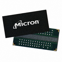
MT47H16M16BG-5E:B Micron Technology Inc, MT47H16M16BG-5E:B Datasheet - Page 108

MT47H16M16BG-5E:B
Manufacturer Part Number
MT47H16M16BG-5E:B
Description
IC DDR2 SDRAM 256MBIT 5NS 84FBGA
Manufacturer
Micron Technology Inc
Datasheet
1.MT47H16M16BG-3B_TR.pdf
(128 pages)
Specifications of MT47H16M16BG-5E:B
Format - Memory
RAM
Memory Type
DDR2 SDRAM
Memory Size
256M (16Mx16)
Speed
5ns
Interface
Parallel
Voltage - Supply
1.7 V ~ 1.9 V
Operating Temperature
0°C ~ 85°C
Package / Case
84-FBGA
Lead Free Status / RoHS Status
Lead free / RoHS Compliant
Available stocks
Company
Part Number
Manufacturer
Quantity
Price
Company:
Part Number:
MT47H16M16BG-5E:B
Manufacturer:
MICRON
Quantity:
121
Company:
Part Number:
MT47H16M16BG-5E:B
Manufacturer:
MICRON
Quantity:
591
Company:
Part Number:
MT47H16M16BG-5E:B
Manufacturer:
Micron Technology Inc
Quantity:
10 000
Company:
Part Number:
MT47H16M16BG-5E:B TR
Manufacturer:
Micron Technology Inc
Quantity:
10 000
Figure 65: Data Input Timing
PRECHARGE
PDF: 09005aef8117c187
256MbDDR2.pdf - Rev. M 7/09 EN
Notes:
DQS#
Precharge can be initiated by either a manual PRECHARGE command or by an autopre-
charge in conjunction with either a READ or WRITE command. Precharge will deacti-
vate the open row in a particular bank or the open row in all banks. The PRECHARGE
operation is shown in the previous READ and WRITE operation sections.
During a manual PRECHARGE command, the A10 input determines whether one or all
banks are to be precharged. In the case where only one bank is to be precharged, bank
address inputs determine the bank to be precharged. When all banks are to be pre-
charged, the bank address inputs are treated as “Don’t Care.”
Once a bank has been precharged, it is in the idle state and must be activated prior to
any READ or WRITE commands being issued to that bank. When a single-bank PRE-
CHARGE command is issued,
mand is issued,
DQS
CK#
DM
DQ
CK
1.
2.
3. Subsequent rising DQS signals must align to the clock within
4. WRITE command issued at T0.
5. For x16, LDQS controls the lower byte and UDQS controls the upper byte.
6. WRITE command with WL = 2 (CL = 3, AL = 0) issued at T0.
t
t
DSH (MIN) generally occurs during
DSS (MIN) generally occurs during
T0
WL - t DQSS (NOM)
t
RPA timing applies, regardless of the number of banks opened.
T1
T1n
t WPRE
108
t
T2
DI
RP timing applies. When the PRECHARGE (ALL) com-
t DSH 1
T2n
t DQSL
t DSS 2
t
t
DQSS (MAX).
DQSS (MIN).
Micron Technology, Inc. reserves the right to change products or specifications without notice.
Transitioning Data
T3
3
t DQSH
256Mb: x4, x8, x16 DDR2 SDRAM
t DSH 1
T3n
t WPST
t DSS 2
T4
Don’t Care
©2003 Micron Technology, Inc. All rights reserved.
t
DQSS.
PRECHARGE


