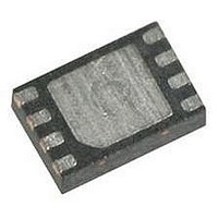
M45PE20-VMP6G NUMONYX, M45PE20-VMP6G Datasheet - Page 23

M45PE20-VMP6G
Manufacturer Part Number
M45PE20-VMP6G
Description
IC FLASH 2MBIT 75MHZ 8VFQFPN
Manufacturer
NUMONYX
Series
Forté™r
Datasheets
1.M45PE20-VMN6TP.pdf
(47 pages)
2.M45PE20-VMN6P.pdf
(34 pages)
3.M45PE20-VMP6G.pdf
(36 pages)
Specifications of M45PE20-VMP6G
Format - Memory
FLASH
Memory Type
FLASH
Memory Size
2M (256K x 8)
Speed
75MHz
Interface
SPI, 3-Wire Serial
Voltage - Supply
2.7 V ~ 3.6 V
Operating Temperature
-40°C ~ 85°C
Package / Case
8-VFQFN, 8-VFQFPN
Memory Configuration
256K X 8
Ic Interface Type
Serial, SPI
Clock Frequency
25MHz
Supply Voltage Range
2.7V To 3.6V
Memory Case Style
VDFPN
No. Of Pins
8
Interface Type
Serial, SPI
Rohs Compliant
Yes
Lead Free Status / RoHS Status
Lead free / RoHS Compliant
Available stocks
Company
Part Number
Manufacturer
Quantity
Price
Part Number:
M45PE20-VMP6G
Manufacturer:
ST
Quantity:
20 000
POWER-UP AND POWER-DOWN
At Power-up and Power-down, the device must
not be selected (that is Chip Select (S) must follow
the voltage applied on V
correct value:
–
–
Usually a simple pull-up resistor on Chip Select (S)
can be used to ensure safe and proper Power-up
and Power-down.
To avoid data corruption and inadvertent write op-
erations during power up, a Power On Reset
(POR) circuit is included. The logic inside the de-
vice is held reset while V
On Reset (POR) threshold value, V
tions are disabled, and the device does not re-
spond to any instruction.
Moreover, the device ignores all Write Enable
(WREN), Page Write (PW), Page Program (PP),
Page Erase (PE) and Sector Erase (SE) instruc-
tions until a time delay of t
the moment that V
old. However, the correct operation of the device
is not guaranteed if, by this time, V
V
should be sent until the later of:
–
Figure 19. Power-up Timing
CC
V
delay of t
V
t
(min). No Write, Program or Erase instructions
PUW
V CC (max)
CC
SS
V CC (min)
(min) at Power-up, and then for a further
at Power-down
after V
V WI
V CC
VSL
CC
Reset State
Device
of the
CC
passed the V
Program, Erase and Write Commands are Rejected by the Device
rises above the V
CC
CC
Chip Selection Not Allowed
) until V
PUW
is less than the Power
has elapsed after
WI
CC
CC
threshold
WI
is still below
reaches the
– all opera-
WI
thresh-
tPUW
tVSL
–
These values are specified in
If the delay, t
above V
READ instructions even if the t
fully elapsed.
As an extra protection, the Reset (Reset) signal
can be driven Low for the whole duration of the
Power-up and Power-down phases.
At Power-up, the device is in the following state:
–
–
Normal precautions must be taken for supply rail
decoupling, to stabilize the V
vice in a system should have the V
pled by a suitable capacitor close to the package
pins. (Generally, this capacitor is of the order of
0.1µF).
At Power-down, when V
ing voltage, to below the Power On Reset (POR)
threshold value, V
and the device does not respond to any instruc-
tion. (The designer needs to be aware that if a
Power-down occurs while a Write, Program or
Erase cycle is in progress, some data corruption
can result.)
Read Access allowed
t
The device is in the Standby Power mode (not
the Deep Power-down mode).
The Write Enable Latch (WEL) bit is reset.
VSL
CC
after V
(min), the device can be selected for
VSL
CC
, has elapsed, after V
passed the V
WI
, all operations are disabled
Device fully
accessible
CC
drops from the operat-
CC
Table
PUW
CC
time
supply. Each de-
(min) level
delay is not yet
CC
6..
CC
M45PE20
AI04009C
rail decou-
has risen
23/35


