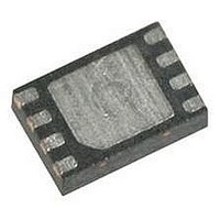
M45PE20-VMP6G NUMONYX, M45PE20-VMP6G Datasheet - Page 8

M45PE20-VMP6G
Manufacturer Part Number
M45PE20-VMP6G
Description
IC FLASH 2MBIT 75MHZ 8VFQFPN
Manufacturer
NUMONYX
Series
Forté™r
Datasheets
1.M45PE20-VMN6TP.pdf
(47 pages)
2.M45PE20-VMN6P.pdf
(34 pages)
3.M45PE20-VMP6G.pdf
(36 pages)
Specifications of M45PE20-VMP6G
Format - Memory
FLASH
Memory Type
FLASH
Memory Size
2M (256K x 8)
Speed
75MHz
Interface
SPI, 3-Wire Serial
Voltage - Supply
2.7 V ~ 3.6 V
Operating Temperature
-40°C ~ 85°C
Package / Case
8-VFQFN, 8-VFQFPN
Memory Configuration
256K X 8
Ic Interface Type
Serial, SPI
Clock Frequency
25MHz
Supply Voltage Range
2.7V To 3.6V
Memory Case Style
VDFPN
No. Of Pins
8
Interface Type
Serial, SPI
Rohs Compliant
Yes
Lead Free Status / RoHS Status
Lead free / RoHS Compliant
Available stocks
Company
Part Number
Manufacturer
Quantity
Price
Part Number:
M45PE20-VMP6G
Manufacturer:
ST
Quantity:
20 000
M45PE20
OPERATING FEATURES
Sharing the Overhead of Modifying Data
To write or program one (or more) data bytes, two
instructions are required: Write Enable (WREN),
which is one byte, and a Page Write (PW) or Page
Program (PP) sequence, which consists of four
bytes plus data. This is followed by the internal cy-
cle (of duration t
To share this overhead, the Page Write (PW) or
Page Program (PP) instruction allows up to 256
bytes to be programmed (changing bits from 1 to
0) or written (changing bits to 0 or 1) at a time, pro-
vided that they lie in consecutive addresses on the
same page of memory.
An Easy Way to Modify Data
The Page Write (PW) instruction provides a con-
venient way of modifying data (up to 256 contigu-
ous bytes at a time), and simply requires the start
address, and the new data in the instruction se-
quence.
The Page Write (PW) instruction is entered by
driving Chip Select (S) Low, and then transmitting
the instruction byte, three address bytes (A23-A0)
and at least one data byte, and then driving Chip
Select (S) High. While Chip Select (S) is being
held Low, the data bytes are written to the data
buffer, starting at the address given in the third ad-
dress byte (A7-A0). When Chip Select (S) is driven
High, the Write cycle starts. The remaining, un-
changed, bytes of the data buffer are automatically
loaded with the values of the corresponding bytes
of the addressed memory page. The addressed
memory page then automatically put into an Erase
cycle. Finally, the addressed memory page is pro-
grammed with the contents of the data buffer.
All of this buffer management is handled internally,
and is transparent to the user. The user is given
the facility of being able to alter the contents of the
memory on a byte-by-byte basis.
A Fast Way to Modify Data
The Page Program (PP) instruction provides a fast
way of modifying data (up to 256 contiguous bytes
at a time), provided that it only involves resetting
bits to 0 that had previously been set to 1.
This might be:
–
–
8/35
when the designer is programming the device
for the first time
when the designer knows that the page has
already been erased by an earlier Page Erase
PW
or t
PP
).
–
Polling During a Write, Program or Erase Cycle
A further improvement in the write, program or
erase time can be achieved by not waiting for the
worst case delay (t
In Progress (WIP) bit is provided in the Status
Register so that the application program can mon-
itor its value, polling it to establish when the previ-
ous cycle is complete.
Reset
An internal Power On Reset circuit helps protect
against inadvertent data writes. Addition protec-
tion is provided by driving Reset (Reset) Low dur-
ing the Power-on process, and only driving it High
when V
V
Active Power, Standby Power and Deep
Power-Down Modes
When Chip Select (S) is Low, the device is select-
ed, and in the Active Power mode.
When Chip Select (S) is High, the device is dese-
lected, but could remain in the Active Power mode
until all internal cycles have completed (Program,
Erase, Write). The device then goes in to the
Standby Power mode. The device consumption
drops to I
The Deep Power-down mode is entered when the
specific instruction (the Deep Power-down (DP) in-
struction) is executed. The device consumption
drops further to I
mode until another specific instruction (the Re-
lease from Deep Power-down and Read Electron-
ic Signature (RES) instruction) is executed.
All other instructions are ignored while the device
is in the Deep Power-down mode. This can be
used as an extra software protection mechanism,
when the device is not in active use, to protect the
device from inadvertent Write, Program or Erase
instructions.
CC
(PE) or Sector Erase (SE) instruction. This is
useful, for example, when storing a fast
stream of data, having first performed the
erase cycle when time was available
when the designer knows that the only
changes involve resetting bits to 0 that are still
set to 1. When this method is possible, it has
the additional advantage of minimising the
number of unnecessary erase operations, and
the extra stress incurred by each page.
(min).
CC
CC1
has reached the correct voltage level,
.
CC2
PW
. The device remains in this
, t
PP
, t
PE
, or t
SE
). The Write


