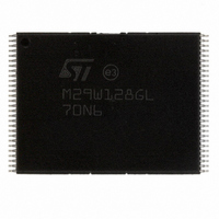
M29W128GL70N6E NUMONYX, M29W128GL70N6E Datasheet - Page 37

M29W128GL70N6E
Manufacturer Part Number
M29W128GL70N6E
Description
IC FLASH 128MBIT 70NS 56TSOP
Manufacturer
NUMONYX
Series
Axcell™r
Datasheet
1.M29W128GH70N6E.pdf
(94 pages)
Specifications of M29W128GL70N6E
Format - Memory
FLASH
Memory Type
FLASH
Memory Size
128M (16Mx8, 8Mx16)
Speed
70ns
Interface
Parallel
Voltage - Supply
2.7 V ~ 3.6 V
Operating Temperature
-40°C ~ 85°C
Package / Case
56-TSOP
Package
56TSOP
Cell Type
NOR
Density
128 Mb
Architecture
Sectored
Block Organization
Symmetrical
Typical Operating Supply Voltage
3|3.3 V
Sector Size
128KByte x 128
Timing Type
Asynchronous
Interface Type
Parallel
Lead Free Status / RoHS Status
Lead free / RoHS Compliant
Available stocks
Company
Part Number
Manufacturer
Quantity
Price
Company:
Part Number:
M29W128GL70N6E
Manufacturer:
MICRON
Quantity:
11 200
Company:
Part Number:
M29W128GL70N6E
Manufacturer:
LATTICE
Quantity:
198
Part Number:
M29W128GL70N6E
Manufacturer:
MICRON
Quantity:
20 000
6.2.4
6.2.5
6.2.6
6.2.7
Write to Buffer Program Confirm command
The Write to Buffer Program Confirm command is used to confirm a Write to Buffer Program
command and to program the N+1 words/bytes loaded in the write buffer by this command.
Enhanced Buffered Program Confirm command
The Enhanced Buffered Program Confirm command is used to confirm an Enhanced
Buffered Program command and to program the 256 words loaded in the buffer.
Unlock Bypass command
The Unlock Bypass command is used to place the device in unlock bypass mode. When the
device enters the unlock bypass mode, the two initial unlock cycles required in the standard
program command sequence are no more needed, and only two write cycles are required to
program data, instead of the normal four cycles (see
This results in a faster total programming time.
Unlock Bypass command is consequently used in conjunction with the Unlock Bypass
Program command to program the memory faster than with the standard program
commands. When the cycle time to the device is long, considerable time saving can be
made by using these commands. Three bus write operations are required to issue the
Unlock Bypass command.
When in unlock bypass mode, only the Unlock Bypass Program, Unlock Bypass Block
Erase, Unlock Bypass Chip Erase, and Unlock Bypass Reset commands are valid:
In unlock bypass mode the memory can be read as if in read mode.
Unlock Bypass Program command
The Unlock Bypass Program command can be used to program one address in the memory
array at a time. The command requires two bus write operations, the final write operation
latches the address and data and starts the program/erase controller.
The program operation using the Unlock Bypass Program command behaves identically to
the program operation using the Program command. The operation cannot be aborted, a
bus read operation to the memory outputs the status register. See the Program command
for details on the behavior.
The Unlock Bypass Program command can be issued to program addresses within the
memory
The Unlock Bypass Block Erase command can then be issued to erase one or more
memory blocks
The Unlock Bypass Chip Erase command can be issued to erase the whole memory
array
The Unlock Bypass Write to Buffer Program command can be issued to speed up
programming operation
The Unlock Bypass Enhanced Buffered Program command can be issued to speed up
programming operation
The Unlock Bypass Reset command can be issued to return the memory to read mode.
Note 5
below
Table 10
and
Table
37/94
11).


