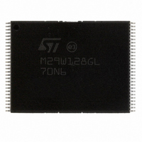
M29W128GL70N6E NUMONYX, M29W128GL70N6E Datasheet - Page 41

M29W128GL70N6E
Manufacturer Part Number
M29W128GL70N6E
Description
IC FLASH 128MBIT 70NS 56TSOP
Manufacturer
NUMONYX
Series
Axcell™r
Datasheet
1.M29W128GH70N6E.pdf
(94 pages)
Specifications of M29W128GL70N6E
Format - Memory
FLASH
Memory Type
FLASH
Memory Size
128M (16Mx8, 8Mx16)
Speed
70ns
Interface
Parallel
Voltage - Supply
2.7 V ~ 3.6 V
Operating Temperature
-40°C ~ 85°C
Package / Case
56-TSOP
Package
56TSOP
Cell Type
NOR
Density
128 Mb
Architecture
Sectored
Block Organization
Symmetrical
Typical Operating Supply Voltage
3|3.3 V
Sector Size
128KByte x 128
Timing Type
Asynchronous
Interface Type
Parallel
Lead Free Status / RoHS Status
Lead free / RoHS Compliant
Available stocks
Company
Part Number
Manufacturer
Quantity
Price
Company:
Part Number:
M29W128GL70N6E
Manufacturer:
MICRON
Quantity:
11 200
Company:
Part Number:
M29W128GL70N6E
Manufacturer:
LATTICE
Quantity:
198
Part Number:
M29W128GL70N6E
Manufacturer:
MICRON
Quantity:
20 000
6.3
6.3.1
Note:
Protection commands
Blocks can be protected individually against accidental program, erase or read operations.
The device block protection scheme is shown in
either
summary of the block protection commands.
Block protection commands are available both in 8-bit and 16-bit configuration.
The memory block and extended memory block protection is configured through the lock
register (see
The program commands referred to in the following sectons must be used according to all
the Program command timings listed here:
Enter Extended Memory Block command
The M29W128GH/L has one extra 128-word block (extended memory block) that can only
be accessed using the Enter Extended Memory Block command.
Three bus write cycles are required to issue the Extended Memory Block command. Once
the command has been issued the device enters the extended memory block mode where
all bus read or program operations are conducted on the extended memory block. Once the
device is in the extended block mode, the extended memory block is addressed by using
the addresses occupied by block 0 in the other operating modes (see
addresses).
The device remains in extended memory block mode until the Exit Extended Memory Block
command is issued or power is removed from the device. After power-up or a hardware
reset, the device reverts to read mode, and the commands issued to block 0 addresses will
properly address block 0.
The extended memory block cannot be erased, and can be treated as one-time
programmable (OTP) memory.
In extended block mode, Erase, Chip Erase, Erase Suspend and Erase Resume commands
are not allowed.
To exit from the extended memory block mode the Exit Extended Memory Block command
must be issued.
The extended memory block can be protected by setting the extended memory block
protection bit to ‘1’ (see
cannot be undone.
When the device is in the extended memory block mode, the V
for fast programming and the unlock bypass mode is not available (see
VPP/write protect
Figure 17.: Write enable controlled program waveforms (8-bit
Figure 18.: Write enable controlled program waveforms (16-bit
Figure 19.: Chip enable controlled program waveforms (8-bit
Figure 20.: Chip enable controlled program waveforms (16-bit
Table
15, or
Section 7.1: Lock
(VPP/WP)).
Table
Section 7.1: Lock
16, depending on the configuration that is being used, for a
register).
register); however once protected the protection
Figure 5: Software protection
PP
/WP pin cannot be used
mode),
mode),
mode).
mode),
Table 35: Block
Section 2.8:
scheme. See
41/94


