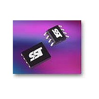
SST25VF040B-50-4I-QAF Microchip Technology, SST25VF040B-50-4I-QAF Datasheet - Page 8

SST25VF040B-50-4I-QAF
Manufacturer Part Number
SST25VF040B-50-4I-QAF
Description
IC FLASH SER 4MB 50MHZ SPI 8WSON
Manufacturer
Microchip Technology
Datasheets
1.SST25VF512A-33-4C-SAE.pdf
(2 pages)
2.SST25VF040B-80-4I-SAE.pdf
(33 pages)
3.SST25VF040B-80-4I-QAE.pdf
(33 pages)
Specifications of SST25VF040B-50-4I-QAF
Memory Type
FLASH
Memory Size
4M (512K x 8)
Operating Temperature
-40°C ~ 85°C
Package / Case
8-WSON
Format - Memory
FLASH
Speed
50MHz
Interface
SPI Serial
Voltage - Supply
2.7 V ~ 3.6 V
Architecture
Sectored
Interface Type
SPI
Access Time
50 ns
Supply Voltage (max)
3.6 V
Supply Voltage (min)
2.7 V
Maximum Operating Current
15 mA
Mounting Style
SMD/SMT
Organization
32 KB
Lead Free Status / RoHS Status
Lead free / RoHS Compliant
Lead Free Status / RoHS Status
Lead free / RoHS Compliant, Lead free / RoHS Compliant
A Microchip Technology Company
©2011 Silicon Storage Technology, Inc.
Auto Address Increment (AAI)
Block Protection (BP3,BP2, BP1, BP0)
Block Protection Lock-Down (BPL)
The Auto Address Increment Programming-Status bit provides status on whether the device is in AAI
programming mode or Byte-Program mode. The default at power up is Byte-Program mode.
The Block-Protection (BP3, BP2, BP1, BP0) bits define the size of the memory area, as defined in
Table 4, to be software protected against any memory Write (Program or Erase) operation. The Write-
Status-Register (WRSR) instruction is used to program the BP3, BP2, BP1 and BP0 bits as long as
WP# is high or the Block-Protect-Lock (BPL) bit is 0. Chip-Erase can only be executed if Block-Protec-
tion bits are all 0. After power-up, BP3, BP2, BP1 and BP0 are set to 1.
WP# pin driven low (V
prevents any further alteration of the BPL, BP3, BP2, BP1, and BP0 bits. When the WP# pin is driven
high (V
0.
Table 4: Software Status Register Block Protection
Protection Level
1. X = Don’t Care (RESERVED) default is “0
2. Default at power-up for BP2, BP1, and BP0 is ‘111’. (All Blocks Protected)
None
Upper 1/8
Upper 1/4
Upper 1/2
All Blocks
All Blocks
All Blocks
All Blocks
IH
), the BPL bit has no effect and its value is “Don’t Care”. After power-up, the BPL bit is reset to
IL
), enables the Block-Protection-Lock-Down (BPL) bit. When BPL is set to 1, it
BP3
X
X
X
X
X
X
X
X
8
Status Register Bit
BP2
0
0
0
0
1
1
1
1
BP1
0
0
1
1
0
0
1
1
4 Mbit SPI Serial Flash
FOR
2
SST25VF040B
BP0
0
1
0
1
0
1
0
1
Protected Memory Address
SST25VF040B
70000H-7FFFFH
60000H-7FFFFH
40000H-7FFFFH
00000H-7FFFFH
00000H-7FFFFH
00000H-7FFFFH
00000H-7FFFFH
1
4 Mbit
None
S71295-06-000
Data Sheet
T4.0 1295
02/11


