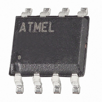
AT25640AN-10SU-2.7 Atmel, AT25640AN-10SU-2.7 Datasheet - Page 9

AT25640AN-10SU-2.7
Manufacturer Part Number
AT25640AN-10SU-2.7
Description
IC EEPROM 64KBIT 20MHZ 8SOIC
Manufacturer
Atmel
Datasheet
1.AT25080A-10PU-2.7.pdf
(26 pages)
Specifications of AT25640AN-10SU-2.7
Format - Memory
EEPROMs - Serial
Memory Type
EEPROM
Memory Size
64K (8K x 8)
Speed
10MHz, 20MHz
Interface
SPI, 3-Wire Serial
Voltage - Supply
2.7 V ~ 5.5 V
Operating Temperature
-40°C ~ 85°C
Package / Case
8-SOIC (3.9mm Width)
Lead Free Status / RoHS Status
Lead free / RoHS Compliant
Other names
AT25640AN-10SU2.7
Available stocks
Company
Part Number
Manufacturer
Quantity
Price
Company:
Part Number:
AT25640AN-10SU-2.7
Manufacturer:
ATMEL
Quantity:
600
Company:
Part Number:
AT25640AN-10SU-2.7
Manufacturer:
ATMEL
Quantity:
300
Part Number:
AT25640AN-10SU-2.7
Manufacturer:
ATMEL/爱特梅尔
Quantity:
20 000
3. Functional Description
3347L–SEEPR–06/07
The AT25080A/160A/320A/640A is designed to interface directly with the synchronous serial
peripheral interface (SPI) of the 6805 and 68HC11 series of microcontrollers.
The AT25080A/160A/320A/640A utilizes an 8-bit instruction register. The list of instructions and
their operation codes are contained in
ferred with the MSB first and start with a high-to-low CS transition.
Table 3-1.
WRITE ENABLE (WREN): The device will power up in the write disable state when V
applied. All programming instructions must therefore be preceded by a Write Enable instruction.
WRITE DISABLE (WRDI): To protect the device against inadvertent writes, the Write Disable
instruction disables all programming modes. The WRDI instruction is independent of the status
of the WP pin.
READ STATUS REGISTER (RDSR): The Read Status Register instruction provides access to
the status register. The READY/BUSY and Write Enable status of the device can be determined
by the RDSR instruction. Similarly, the Block Write Protection Bits indicate the extent of protec-
tion employed. These bits are set by using the WRSR instruction.
Table 3-2.
Instruction Name
WREN
WRDI
RDSR
WRSR
READ
WRITE
WPEN
Bit 7
Instruction Set for the AT25080A/160A/320A/640A
Status Register Format
Bit 6
X
Instruction Format
0000 X110
0000 X100
0000 X101
0000 X001
0000 X011
0000 X010
Bit 5
X
Bit 4
Table
X
AT25080A/160A/320A/640A
3-1. All instructions, addresses, and data are trans-
Bit 3
BP1
Operation
Set Write Enable Latch
Reset Write Enable Latch
Read Status Register
Write Status Register
Read Data from Memory Array
Write Data to Memory Array
Bit 2
BP0
WEN
Bit 1
Bit 0
RDY
CC
is
9


