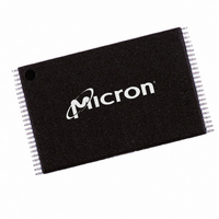
MT29F2G08AABWP Micron Technology Inc, MT29F2G08AABWP Datasheet - Page 10

MT29F2G08AABWP
Manufacturer Part Number
MT29F2G08AABWP
Description
IC FLASH 2GBIT 48TSOP
Manufacturer
Micron Technology Inc
Datasheet
1.MT29F2G08AAAWP.pdf
(57 pages)
Specifications of MT29F2G08AABWP
Format - Memory
FLASH
Memory Type
FLASH - Nand
Memory Size
2G (256M x 8)
Interface
Parallel
Voltage - Supply
2.7 V ~ 3.6 V
Operating Temperature
0°C ~ 70°C
Package / Case
48-TSOP
Lead Free Status / RoHS Status
Lead free / RoHS Compliant
Speed
-
Other names
557-1148-2
Available stocks
Company
Part Number
Manufacturer
Quantity
Price
Company:
Part Number:
MT29F2G08AABWP:B
Manufacturer:
MICRON
Quantity:
2 000
Architecture
Addressing
PDF: 09005aef818a56a7 / Source: 09005aef81590bdd
2gb_nand_m29b__2.fm - Rev. I 1/06 EN
These devices use NAND electrical and command interfaces. Data, commands, and
addresses are multiplexed onto the same pins. This provides a memory device with a
low pin count.
The internal memory array is accessed on a page basis. When doing reads, a page of data
is copied from the memory array into the data register. Once copied to the data register,
data is output sequentially, byte-by-byte on x8 devices, or word-by-word on x16 devices.
The memory array is programmed on a page basis. After the starting address is loaded
into the internal address register, data is sequentially written to the internal data register
up to the end of a page. After all of the page data has been loaded into the data register,
array programming is started.
In order to increase programming bandwidth, this device incorporates a cache register.
In the cache programming mode, data is first copied into the cache register and then
into the data register. Once the data is copied into the data register, programming
begins.
After the data register has been loaded and programming started, the cache register
becomes available for loading additional data. Loading the next page of data into the
cache register takes place while page programming is in process.
The INTERNAL DATA MOVE command also uses the internal cache register. Normally,
moving data from one area of external memory to another uses a large number of exter-
nal memory cycles. By using the internal cache register and data register, array data can
be copied from one page and then programmed into another without using external
memory cycles.
NAND Flash devices do not contain dedicated address pins. Addresses are loaded using
a five-cycle sequence as shown in Figures 7 and 8, on pages 12 and 13 respectively.
Table 2 on page 12 presents address functions internal to the x8 device; Table 3 on
page 13 covers the same functions for the x16 device. See Figures 5 and 6 on page 11 for
additional memory mapping and addressing details.
2, 4, 8Gb: x8/x16 Multiplexed NAND Flash Memory
10
Micron Technology, Inc., reserves the right to change products or specifications without notice.
©2004 Micron Technology, Inc. All rights reserved.
Architecture


