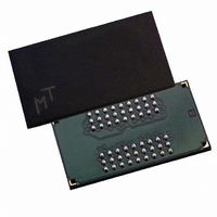
MT48H4M16LFB4-8 IT Micron Technology Inc, MT48H4M16LFB4-8 IT Datasheet - Page 10

MT48H4M16LFB4-8 IT
Manufacturer Part Number
MT48H4M16LFB4-8 IT
Description
IC SDRAM 64MBIT 125MHZ 54VFBGA
Manufacturer
Micron Technology Inc
Datasheet
1.MT48H4M16LFB4-10.pdf
(54 pages)
Specifications of MT48H4M16LFB4-8 IT
Format - Memory
RAM
Memory Type
Mobile SDRAM
Memory Size
64M (4M x 16)
Speed
125MHz
Interface
Parallel
Voltage - Supply
1.7 V ~ 1.9 V
Operating Temperature
-40°C ~ 85°C
Package / Case
54-VFBGA
Lead Free Status / RoHS Status
Lead free / RoHS Compliant
CAS Latency
between the registration of a READ command and the
availability of the first piece of output data. The latency
can be set to one, two, or three clocks.
and the latency is m clocks, the data will be available
by clock edge n + m. The DQs will start driving as a
result of the clock edge one cycle earlier (n + m - 1),
and provided that the relevant access times are met,
the data will be valid by clock edge n + m. For example,
assuming that the clock cycle time is such that all rele-
vant access times are met, if a read command is regis-
tered at T0 and the latency is programmed to two
clocks, the DQs will start driving after T1 and the data
will be valid by T2, as shown in Figure 5, CAS Latency.
Table 5, indicates the operating frequencies at which
each CAS latency setting can be used.
operation or incompatibility with future versions may
result.
pdf: 09005aef80a63953, source: 09005aef808a7edc
Y25L_64Mb_2.fm - Rev. E 11/04 EN
COM MAND
COM MAND
The CAS latency is the delay, in clock cycles,
If a READ command is registered at clock edge n,
Reserved states should not be used as unknown
CLK
CLK
DQ
DQ
READ
READ
T0
T0
Figure 5: CAS Latency
CAS Latency = 2
NOP
NOP
T1
T1
t
t AC
LZ
CAS Latency = 3
T2
T2
NOP
NOP
t
t AC
LZ
D
t OH
OUT
T3
T3
NOP
D
t OH
OUT
DON’T CARE
UNDEFINED
T4
10
Table 5:
Operating Mode
M7 and M8 to zero; the other combinations of values
for M7 and M8 are reserved for future use and/or test
modes. The programmed burst length applies to both
read and write bursts.
because unknown operation or incompatibility with
future versions may result.
Write Burst Mode
M2 applies to both READ and WRITE bursts; when M9
= 1, the programmed burst length applies to READ
bursts, but write accesses are single-location (non-
burst) accesses.
Extended Mode Register
beyond those controlled by the mode register. These
additional functions are special features of the mobile
device. They include temperature compensated self
refresh (TCSR) control, partial array self refresh (PASR),
and output drive strength. Not programming the
extended mode register upon initialization, will result
in default settings for the low power features. The
extended mode will default to the +85 C setting for
TCSR, full drive strength, and full array refresh.
MODE REGISTER SET command (BA1 = 1, BA0 = 0)
and retains the stored information until it is pro-
grammed again or the device loses power.
with E6 through E11 set to “0.” It must be loaded when
all banks are idle and no bursts are in progress, and the
controller must wait the specified time before initiat-
ing any subsequent operation. Violating either of these
requirements results in unspecified operation.
ister settings will be retained even after exiting deep
power-down.
The normal operating mode is selected by setting
Test modes and reserved states should not be used
When M9 = 0, the burst length programmed via M0-
The extended mode register controls the functions
The extended mode register is programmed via the
The extended mode register must be programmed
Once the values are entered the extended mode reg-
SPEED
-10
-8
Micron Technology, Inc., reserves the right to change products or specifications without notice.
CAS LATENCY = 2
CAS Latency
ALLOWABLE OPERATING
83.3
104
FREQUENCY (MHZ)
MOBILE SDRAM
©2003 Micron Technology, Inc. All rights reserved.
CAS LATENCY = 3
64Mb: x16
125
104


