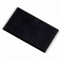
M29W200BB90N1 STMicroelectronics, M29W200BB90N1 Datasheet - Page 2

M29W200BB90N1
Manufacturer Part Number
M29W200BB90N1
Description
IC FLASH 2MBIT 90NS 48TSOP
Manufacturer
STMicroelectronics
Datasheet
1.M29W200BB55N1.pdf
(22 pages)
Specifications of M29W200BB90N1
Format - Memory
FLASH
Memory Type
FLASH - Nor
Memory Size
2M (256K x 8 or 128K x 16)
Speed
90ns
Interface
Parallel
Voltage - Supply
2.7 V ~ 3.6 V
Operating Temperature
0°C ~ 70°C
Package / Case
48-TSOP
Lead Free Status / RoHS Status
Lead free / RoHS Compliant
Available stocks
Company
Part Number
Manufacturer
Quantity
Price
Company:
Part Number:
M29W200BB90N1
Manufacturer:
ST
Quantity:
1 200
Company:
Part Number:
M29W200BB90N1/90N6
Manufacturer:
NEC
Quantity:
2 500
Part Number:
M29W200BB90N1/90N6
Manufacturer:
ST
Quantity:
20 000
M29W200BT, M29W200BB
Figure 2. TSOP Connections
Table 1. Signal Names
2/22
A0-A16
DQ0-DQ7
DQ8-DQ14
DQ15A–1
E
G
W
RP
RB
BYTE
V
V
NC
CC
SS
A15
A14
A13
A12
A11
A10
NC
NC
NC
NC
NC
NC
RP
RB
A9
A8
A7
A6
A5
A4
A3
A2
A1
W
1
12
13
24
Address Inputs
Data Inputs/Outputs
Data Inputs/Outputs
Data Input/Output or Address Input
Chip Enable
Output Enable
Write Enable
Reset/Block Temporary Unprotect
Ready/Busy Output
Byte/Word Organization Select
Supply Voltage
Ground
Not Connected Internally
M29W200BB
M29W200BT
AI02944
48
37
36
25
A16
BYTE
V SS
DQ15A–1
DQ7
DQ14
DQ6
DQ13
DQ5
DQ12
DQ4
V CC
DQ11
DQ3
DQ10
DQ2
DQ9
DQ1
DQ8
DQ0
G
V SS
E
A0
Figure 3. SO Connections
SUMMARY DESCRIPTION
The M29W200B is a 2 Mbit (256Kb x8 or 128Kb
x16) non-volatile memory that can be read, erased
and reprogrammed. These operations can be per-
formed using a single low voltage (2.7 to 3.6V)
supply. On power-up the memory defaults to its
Read mode where it can be read in the same way
as a ROM or EPROM. The M29W200B is fully
backward compatible with the M29W200.
The memory is divided into blocks that can be
erased independently so it is possible to preserve
valid data while old data is erased. Each block can
be protected independently to prevent accidental
Program or Erase commands from modifying the
memory. Program and Erase commands are writ-
ten to the Command Interface of the memory. An
on-chip Program/Erase Controller simplifies the
process of programming or erasing the memory by
taking care of all of the special operations that are
required to update the memory contents. The end
of a program or erase operation can be detected
and any error conditions identified. The command
set required to control the memory is consistent
with JEDEC standards.
DQ10
DQ11
DQ0
DQ8
DQ1
DQ9
DQ2
DQ3
V SS
NC
NC
RB
A7
A6
A5
A4
A3
A2
A1
A0
G
E
1
2
3
4
5
6
7
8
9
10
11
12
13
14
15
16
17
18
19
20
21
22
M29W200BB
M29W200BT
AI02945
44
43
42
41
40
39
38
37
36
35
34
33
32
31
30
29
28
27
26
25
24
23
RP
W
A8
A9
A10
A11
A12
A13
A14
A15
A16
BYTE
V SS
DQ15A–1
DQ7
DQ14
DQ6
DQ13
DQ5
DQ12
DQ4
V CC


