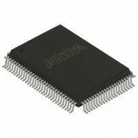
EPC4QI100 Altera, EPC4QI100 Datasheet - Page 76

EPC4QI100
Manufacturer Part Number
EPC4QI100
Description
IC CONFIG DEVICE 4MBIT 100-PQFP
Manufacturer
Altera
Series
EPCr
Datasheet
1.EPC4QI100N.pdf
(116 pages)
Specifications of EPC4QI100
Programmable Type
In System Programmable
Memory Size
4Mb
Voltage - Supply
3 V ~ 3.6 V
Operating Temperature
-40°C ~ 85°C
Package / Case
100-MQFP, 100-PQFP
Lead Free Status / RoHS Status
Contains lead / RoHS non-compliant
Other names
544-2189
Available stocks
Company
Part Number
Manufacturer
Quantity
Price
Company:
Part Number:
EPC4QI100
Manufacturer:
ALTERA
Quantity:
1
Part Number:
EPC4QI100
Manufacturer:
ALTERA/阿尔特拉
Quantity:
20 000
Company:
Part Number:
EPC4QI100N
Manufacturer:
ALTERA
Quantity:
300
Part Number:
EPC4QI100N
Manufacturer:
ALTERA/阿尔特拉
Quantity:
20 000
3–24
Figure 3–15. Write Bytes Operation Timing Diagram
Notes to
(1) Use the erase sector or the erase bulk instruction to initialize the memory bytes of the serial configuration devices to all 1 or 0xFF before
(2) Address bit A[23] is a don't-care bit in EPCS64. Address bits A[23..21] are don't-care bits in EPCS16. Address bits A[23..19] are
(3) For .rpd files, write the LSB of the data byte first.
Configuration Handbook (Complete Two-Volume Set)
DCLK
ASDI
nCS
implementing the write bytes operation.
don't-care bits in EPCS4. Address bits A[23..17] are don't-care bits in EPCS1.
Figure
0
1
2
3–15:
Operation Code
1
3
4
5
If the design must write more than 256 data bytes to the memory, it needs more than
one page of memory. Send the write enable and write bytes operation codes followed
by three new targeted address bytes and 256 data bytes before a new page is written.
nCS must be driven high after the eighth bit of the last data byte has been latched in.
Otherwise, the device will not execute the write bytes operation. The write enable
latch bit in the status register is reset to 0 before the completion of each write bytes
operation. Therefore, the write enable operation must be carried out before the next
write bytes operation.
The device initiates the self-timed write cycle immediately after nCS is driven high.
Refer to t
respective EPCS devices. Therefore, you must account for this amount of delay before
another page of memory is written. Alternatively, you can check the status register’s
write in progress bit by executing the read status operation while the self-timed write
cycle is in progress. The write in progress bit is set to 1 during the self-timed write
cycle, and 0 when it is complete.
The bytes of serial configuration devices memory must be erased to all 1 or 0xFF
before write bytes operation is implemented. This can be achieved by either using the
erase sector instruction in a sector, or the erase bulk instruction throughout the entire
memory.
Erase Bulk Operation
The erase bulk operation code is b'1100 0111, with the MSB listed first. The erase
bulk operation sets all memory bits to 1 or 0xFF. Similar to the write bytes operation,
the write enable operation must be executed prior to the erase bulk operation so that
the write enable latch bit in the status register is set to 1.
You can implement the erase bulk operation by driving nCS low and then shifting in
the erase bulk operation code on the ASDI pin. nCS must be driven high after the
eighth bit of the erase bulk operation code has been latched in.
timing diagram.
The device initiates the self-timed erase bulk cycle immediately after nCS is driven
high. Refer to t
respective EPCS devices.
6
7
MSB
23
8
22
9
21
10
WB
24-Bit Address (2)
Chapter 3: Serial Configuration Devices (EPCS1, EPCS4, EPCS16, EPCS64, and EPCS128) Data Sheet
in
Table 3–16 on page 3–27
EB
3
28
in
2
29
Table 3–16
1
30
0
31
MSB (3)
7
32
(Note 1)
6
33
5
34
for the self-timed erase bulk cycle time for the
Data Byte 1
4
35
3
36
2
37
1
38
for the self-timed write cycle time for the
0
39
MSB (3)
7
40
6
41
5
42
Data Byte 2
4
43
44
3
2
45
Serial Configuration Device Memory Access
1
46
© December 2009
0
47
Figure 3–16
MSB (3)
2072 2073 2074 2075 2076 2077 2078 2079
7
6
5
Data Byte 256
Altera Corporation
4
shows the
3
2
1
0


