EPC1213LC20 Altera, EPC1213LC20 Datasheet
EPC1213LC20
Specifications of EPC1213LC20
Available stocks


Related parts for EPC1213LC20


EPC1213LC20 Summary of contents
Page 1
... This section provides information about Altera chapters contain information about how to use these devices, feature descriptions, device pin tables, and package diagrams. This section includes the following chapters: ■ Chapter 1, Enhanced Configuration Devices (EPC4, EPC8, and EPC16) Data Sheet ■ Chapter 2, Altera Enhanced Configuration Devices ■ ...
Page 2
... I–2 Configuration Handbook (Complete Two-Volume Set) Section I: FPGA Configuration Devices Revision History © December 2009 Altera Corporation ...
Page 3
... Supports byte-wide configuration mode fast passive parallel (FPP); 8-bit data output per DCLK cycle ■ Supports true n-bit concurrent configuration ( and 8) of Altera FPGAs Pin-selectable 2-ms or 100-ms power-on reset (POR) time ■ ■ Configuration clock supports programmable input source and frequency synthesis Multiple configuration clock sources supported (internal oscillator and ■ ...
Page 4
... The flash memory is used to store configuration data for systems made up of one or more Altera FPGAs. Unused portions of the flash memory can be used to store processor code or data that can be accessed via the external flash interface after FPGA configuration is complete ...
Page 5
... Chapter 1: Enhanced Configuration Devices (EPC4, EPC8, and EPC16) Data Sheet Functional Description Table 1–2. Configuration Devices Required (Part Family Arria GX Stratix Stratix GX Stratix II Stratix II GX Cyclone © December 2009 Altera Corporation Data Size (Bits) Device (1) EPC4 EP1AGX20C 9,640,672 EP1AGX35C 9,640,672 EP1AGX35D ...
Page 6
... EP2A15 4,358,512 EP2A25 6,275,200 EP2A40 9,640,528 EP2A70 17,417,088 EPF10K10 118,000 EPF10K20 231,000 EPF10K30 376,000 EPF10K40 498,000 EPF10K50 621,000 EPF10K70 892,000 EPF10K100 1,200,000 Functional Description (2) EPC8 (2) EPC16 ( — — — — — — — — — © December 2009 Altera Corporation ...
Page 7
... Memory-Based EPC4, EPC8 and EPC16 Devices EPC devices support three different types of flash memory. supported flash memory for all EPC devices. Table 1–3. Enhanced Configuration Devices Flash Memory (Part Device EPC4 EPC8 © December 2009 Altera Corporation Data Size (Bits) Device (1) EPF10K10A 120,000 EPF10K30A ...
Page 8
... Source for EPC4, EPC8 and EPC16 Enhanced Configuration The external flash interface is currently supported in the EPC16 and EPC4 devices. For information about using this feature in the EPC8 device, contact Altera Applica- tions at www.altera.com/support. Enhanced configuration devices have a 3.3-V core and I/O interface. The controller chip is a synchronous system that implements the various interfaces and features. Figure 1– ...
Page 9
... DCLK and DATA[] output pins. The controller selects the configuration page to be transmitted to the FPGA by sampling its PGM[2..0] pins after POR or reset. © December 2009 Altera Corporation Remote chapter in the Stratix Device Configuration Handbook (Complete Two-Volume Set) ...
Page 10
... MHz). Hence, the flash read bandwidth is limited to about 160 megabits per second (Mbps) (16-bit flash data bus, DQ[], at 10 MHz). However, the configuration speeds supported by Altera FPGAs are much higher and translate to high configuration write bandwidths. For instance, 100-MHz Stratix FPP configuration requires data at the rate of 800 Mbps (8-bit DATA[] bus at 100 MHz) ...
Page 11
... Chapter 1: Enhanced Configuration Devices (EPC4, EPC8, and EPC16) Data Sheet Functional Description Configuration Signals Table 1–4 lists the configuration signal connections between the enhanced configuration device and Altera FPGAs. Table 1–4. Configuration Signals Enhanced Configuration Device Pin DATA[] DCLK nINIT_CONF, which ...
Page 12
... While Altera FPGAs can be cascaded in a configuration chain, the enhanced configuration devices cannot be cascaded to configure larger devices or chains. Configuration Handbook (Complete Two-Volume Set) Chapter 1: Enhanced Configuration Devices (EPC4, EPC8, and EPC16) Data Sheet ...
Page 13
... PS mode using an enhanced configuration device. f For specific details about configuration interface connections including pull-up resistor values, supply voltages, and MSEL pin settings, refer to the appropriate FPGA family chapter in the © December 2009 Altera Corporation Configuration Handbook. Configuration Handbook (Complete Two-Volume Set) 1–11 ...
Page 14
... TM0 to GND, and WP supply from V . For more information, refer section CCW CC Functional Description Device WE#F RP#F N.C. A[20..0] N.C. RY/BY# N.C. CE# N.C. OE# N.C. DQ[15..0] (3) V (7) CC VCCW (4) PORSEL (4) PGM[2..0] EXCLK (4) A0-F A1-F A15-F A16-F “Intel-Flash-Based EPC © December 2009 Altera Corporation ...
Page 15
... Since the internal flash interface is directly connected to the external flash interface pins, controller flash access cycles will toggle the external flash interface pins. The external device must be able to tri-state its flash interface during these operations and ignore transitions on the flash interface pins. © December 2009 Altera Corporation Mode (n =) (1) Used Outputs ...
Page 16
... For the Intel Advanced Boot Block Flash Memory (B3) 28F008/800B3, 28F016/160B3, 28F320B3, 28F640B3 Datasheet, visit www.intel.com. Configuration Handbook (Complete Two-Volume Set) Chapter 1: Enhanced Configuration Devices (EPC4, EPC8, and EPC16) Data Sheet Altera Enhanced Configuration Devices Functional Description chapter in volume 2 of the © December 2009 Altera Corporation ...
Page 17
... Figure 1–4: (1) For external flash interface support in EPC8 enhanced configuration device, contact Altera Applications. (2) Pin A20 in EPC16 devices, pins A20 and A19 in EPC8 devices, and pins A20, A19, and A18 in EPC4 devices should be left floating. These pins should not be connected to any signal; they are no-connect pins. ...
Page 18
... < V until V is fully powered up. PP PPLK powered up. PP < PPLK . CC should reach the minimum V CC Functional Description disables writes. PPLK is a programming PP is equivalent to the VCCW pin on PP before 50 ms and RP# CC © December 2009 Altera Corporation ...
Page 19
... For detailed information about the page-mode feature implementation and programming file generation steps using the Quartus II software, refer to the Enhanced Configuration Devices © December 2009 Altera Corporation in the Stratix Device Handbook. chapter in volume 2 of the Configuration Handbook. Configuration Handbook (Complete Two-Volume Set) 1– ...
Page 20
... These unused routing and logic resources as well as un-initialized memory structures result in a large number of configuration RAM bits in the disabled state. Altera's proprietary compression algorithm takes advantage of such bitstream qualities. The general guideline for effectiveness of compression is the higher the device ...
Page 21
... External Clock (Up to 100 MHz) The DCLK frequency is limited by the maximum DCLK frequency the FPGA supports. f The maximum DCLK input frequency supported by the FGPA is specified in the appropriate FPGA family chapter in the © December 2009 Altera Corporation (Note 1) Minimum 98% 1.9 47% Figure 1–5 ...
Page 22
... Chapter 1: Enhanced Configuration Devices (EPC4, EPC8, and EPC16) Data Sheet Table 1–7. Min (MHz) Typ (MHz) 6.4 8.0 21.0 26.5 32.0 40.0 42.0 53.0 Altera Enhanced Configuration Devices © December 2009 Altera Corporation Functional Description Max (MHz) 10.0 33.0 50.0 66.0 chapter in volume 2 ...
Page 23
... Pin Name Pin Type Output DATA[7..0] Output DCLK © December 2009 Altera Corporation Table 1–10 describe the enhanced configuration device pins. These Description Configuration data output bus. DATA changes on each falling edge of DCLK. DATA is latched into the FPGA on the rising edge of DCLK. ...
Page 24
... Active low flash input pin that activates the flash memory when asserted. When it is high, it deselects the device and reduces power consumption to standby levels. This flash input pin is internally connected to the controller. Leave this pin floating on the board when the external flash interface is not used. Pin Description © December 2009 Altera Corporation ...
Page 25
... Supply CCW Open-Drain Output RY/BY# © December 2009 Altera Corporation Description Active low flash input pin that resets the flash when asserted. When high, it enables normal operation. When low, it inhibits write operation to the flash memory, which provides data protection during power transitions. ...
Page 26
... This pin must be connected to a valid logic level. For normal operation, this test pin must be connected to GND. For normal operating, this test pin must be connected to V Pin Description of the Intel flash die CCQ without using any CC white paper © December 2009 Altera Corporation ...
Page 27
... FPGA detects a CRC error or if the FPGA’s nCONFIG input pin is asserted ■ The controller detects a configuration error and asserts OE to begin re-configuration of the Altera FPGA (for example, when CONF_DONE stays low after all configuration data has been transmitted) Power Sequencing Altera requires that you power-up the FPGA's V configuration device's POR expires ...
Page 28
... Selects the USERCODE register and places it between TDI and TDO, allowing the USERCODE to be serially shifted out the TDO. The 32-bit USERCODE is a programmable user-defined pattern. Programming and Configuration File Support Altera Enhanced section in volume 2 of the © December 2009 Altera Corporation ...
Page 29
... Intel HEX format file (.hexout) using the Quartus II Convert Programming Files utility, for use with the programmers or processors. You can also program the enhanced configuration devices using the Quartus II software, the Altera Programming Unit (APU), and the appropriate configuration device programming adapter. with each enhanced configuration device. ...
Page 30
... JPSU JPH t t JPZX JPCO t t JSSU JSH t t JSZX JSCO JSXZ Parameter IEEE Std. 1149.1 (JTAG) Boundary-Scan t JPXZ Min Max Unit 100 — — — — — ns — — — — — ns — — — © December 2009 Altera Corporation ...
Page 31
... For more information about the flash memory (external flash interface) timing, refer to the appropriate flash data sheet on the Altera website at www.altera.com. ■ For Micron flash-based EPC4, refer to the Micron MT28F400B3 Data Sheet Flash Memory Used in EPC4 Devices at For Sharp flash-based EPC16, refer to the Sharp LHF16J06 Data Sheet Flash Memory ■ ...
Page 32
... Min Max Unit -0.2 4.6 V -0.5 3.6 V — 100 mA - — 360 mW -65 150 C -65 135 C — 135 C Min Max Unit 3.0 3.6 V –0 0 – — — © December 2009 Altera Corporation ...
Page 33
... I V supply current CCW CCW Note to Table 1–18: (1) For V supply current information, refer to the appropriate flash memory data sheet at www.altera.com. CCW Table 1–19. Enhanced Configuration Device Capacitance Symbol Parameter CIN Input pin capacitance COUT Output pin capacitance Package The EPC16 enhanced configuration device is available in both the 88-pin UFBGA package and the 100-pin PQFP package ...
Page 34
... Pin pin for Intel Flash-based EPC16. Package Layout Recommendation Sharp flash-based EPC16 and EPC8 enhanced configuration devices in the 100-pin PQFP packages have different package dimensions than other Altera 100-pin PQFP devices (including the Micron flash-based EPC4, Intel flash-based EPC16, EPC8 and EPC4). ...
Page 35
... Used 0.3-mm increase to maximum foot width. f For package outline drawings, refer to the Device Pin-Outs f For pin-out information, refer to © December 2009 Altera Corporation 0.65-mm Pad Pitch 0.410 mm 25.3 mm Altera Device Package Information Data Altera Configuration Devices Pin-Out Configuration Handbook (Complete Two-Volume Set) 1– ...
Page 36
... Updated VCCW connection in Figure 2–2, Figure 2–3, and Figure 2–4. Updated (Note 2) of Figure 2–2, Figure 2–3, and Figure 2–4. Updated (Note 4) of Table 2–12. Updated unit of ICC0 in Table 2–16. Added ICCW to Table 2–16. Initial Release. Chapter Revision History © December 2009 Altera Corporation ...
Page 37
... Object File (.sof) to use Bit0 in the Quartus II software, that .sof will be transmitted on the DATA[0] line from the enhanced configuration device to the SRAM-based device. Supported Schemes and Guidelines There are several different ways to configure Altera SRAM-based programmable logic devices (PLDs) with enhanced configuration devices: ■ 1-bit passive serial (PS) ■ ...
Page 38
... SRAM-based devices or device chains. In addition, these devices do not have to be the same device family or density; they can be any combination of Altera SRAM-based devices. An individual enhanced configuration device DATA line is available for each targeted device. Each DATA line can also feed a daisy chain of devices ...
Page 39
... Chapter 2: Altera Enhanced Configuration Devices Concurrent Configuration Figure 2–1. Software Settings for Configuring Devices Using Alternatively, you can daisy chain two SRAM-based devices to one DATA line while the other DATA lines drive one device each. For example, you could use the 2-bit PS mode to drive two SRAM-based devices with DATA Bit0 (EP20K100E and EP20K60E devices) and the third device (the EP20K200E device) with DATA Bit1 ...
Page 40
... Figure 2–2. Daisy Chaining Two SRAM-Based Devices to One DATA Line Design Guidelines For debugging, Altera recommends keeping the control lines such as nSTATUS, nCONFIG, and CONF_DONE between each PLD and the configuration device separate. You can keep control lines separate with a switch to manage which control signals are fed back into the enhanced configuration device ...
Page 41
... PLD that only processes data packets; page 1 could contain a configuration file for the same PLD that processes data and voice packets. With the ability to dynamically switch pages, you can also configure Altera devices with various revisions for debugging without having to reprogram the configuration device. For example, you can configure a device that is on “ ...
Page 42
... If you choose one of these modes, the Quartus II software reports an error message when the .pof is generated. Configuration Handbook (Complete Two-Volume Set) Chapter 2: Altera Enhanced Configuration Devices Dynamic Configuration (Page Mode) Implementation Overview Page register residing in the flash memory PAGE7_ADDR ...
Page 43
... Chapter 2: Altera Enhanced Configuration Devices Dynamic Configuration (Page Mode) Implementation Overview In the Convert Programming Files window, there are SOF Data entries (.sof), located in the Input files to convert dialog box. Each SOF Data entry refers to a unique system configuration. device and uses two pages, 0 and 1. Each page has a different version of the configuration file for the same APEX device. Figure 2– ...
Page 44
... You can use the flash memory to store boot or application code for processors general-purpose memory for processors and PLDs. Configuration Handbook (Complete Two-Volume Set) Chapter 2: Altera Enhanced Configuration Devices External Flash Memory Interface © December 2009 Altera Corporation ...
Page 45
... Stratix & Stratix GX Devices Upgrades with Stratix II & Stratix II GX Devices Currently, EPC4 and EPC16 configuration devices support the external flash interface. For support of this feature in other enhanced configuration devices, contact Altera Applications. Flash Memory Map You can divide an enhanced configuration device’s flash memory into two categories: logical (configuration and processor space) and physical (flash data block boundaries) ...
Page 46
... For Sharp flash-based EPC16, refer to the Sharp LHF16J06 Data Sheet Flash Memory Used in EPC16 Devices at www.sharpsma.com. ■ For the Intel Advanced Boot Block Flash Memory (B3) 28F008/800B3, 28F016/160B3, 28F320B3, 28F640B3 Datasheet, visit www.intel.com. Configuration Handbook (Complete Two-Volume Set) Chapter 2: Altera Enhanced Configuration Devices Flash Memory Map Processor Application Code Specifications Unused Memory ...
Page 47
... Chapter 2: Altera Enhanced Configuration Devices External Flash Memory Interface Interface Availability and Connections Flash memory ports are shared between the internal controller and the external device. A processor or PLD can use the external flash interface to access flash memory only when the controller is not using the interface. Therefore, the internal controller is the primary master of the bus, while the external device is the secondary master ...
Page 48
... The .map file contains starting and ending addresses for boot code, configuration page data, and application code. Configuration Handbook (Complete Two-Volume Set) Chapter 2: Altera Enhanced Configuration Devices External Flash Memory Interface © December 2009 Altera Corporation ...
Page 49
... Chapter 2: Altera Enhanced Configuration Devices Data Compression You can use the .hexout to program blank enhanced configuration devices, update portions of the flash memory (for example, a new configuration page), or both. This file uses the Intel hexadecimal file format and contains 16 Mbits or 2 Mbytes of data. ...
Page 50
... MHz. The minimum and maximum speeds are shown in the Configuration Device Data accept an external clock source running at speeds 100 MHz. Configuration Handbook (Complete Two-Volume Set) Chapter 2: Altera Enhanced Configuration Devices Configuration Sheet. Additionally, the enhanced configuration device can © December 2009 Altera Corporation ...
Page 51
... Chapter 2: Altera Enhanced Configuration Devices Conclusion Figure 2–13. Clock Divider Unit in Enhanced Configuration Devices External Clock (Up to 100 MHz) Software Implementations You can select the clock source and the clock speed in the Programming Object File Options window with pof selected as the programming file type (Convert ...
Page 52
... September 2003 1.0 ■ Configuration Handbook (Complete Two-Volume Set) Chapter 2: Altera Enhanced Configuration Devices Changes Made Removed “Referenced Documents” section. Added “Referenced Documents” section. Updated new document format. Added document revision history. Technical content added. Added text regarding pointing to an incorrect page after Renamed ...
Page 53
... BP Microsystems, System General, and other vendors ■ Delivered with the memory array erased (all the bits set The term “serial configuration devices” used in this document refers to Altera EPCS1, EPCS4, EPCS16, EPCS64, and EPCS128. © December 2009 Altera Corporation 3. Serial Configuration Devices (EPCS1, EPCS4, EPCS16, EPCS64, and EPCS128) ® ...
Page 54
... Notes to Table 3–1: (1) To program these devices using Altera Programming Unit or Master Programming Unit, refer to (2) The EPCS device can be re-programmed in system with Byte Blaster II download cable or an external microprocessor using SRunner. For more information about SRunner, refer to the AN418, SRunner: An Embedded Solution for EPCS For an 8-pin SOIC package, you can migrate vertically from the EPCS1 to the EPCS4 or EPCS16 because the EPCS devices are offered in the same device package ...
Page 55
... For more information about accessing memory within the serial configuration device, refer to the Active Serial Memory Interface Data Active Serial FPGA Configuration The following Altera FPGAs support Active Serial (AS) configuration scheme with serial configuration devices: Arria series ■ ■ Cyclone series ■ ...
Page 56
... Connect the FPGA MSEL[] input pins to select the AS configuration mode. For details, refer to the respective FPGA family chapter in the Configuration Handbook. (4) For more information about configuration pin I/O requirements scheme for an Altera FPGA, refer to the respective FPGA family handbook Configuration chapter. Configuration Handbook (Complete Two-Volume Set) ...
Page 57
... Connect the FPGA MSEL[] input pins to select the AS configuration mode. For details, refer to the respective FPGA family chapter in the Configuration Handbook. (4) For more information about configuration pin I/O requirements scheme for an Altera FPGA, refer to the respective FPGA family handbook Configuration chapter.. The FPGA acts as the configuration master in the configuration flow and provides the clock to the serial configuration device ...
Page 58
... Connect the FPGA MSEL[] input pins to select the PS configuration mode. For details, refer to the appropriate FPGA family chapter in the Configuration Handbook. (5) For more information about configuration pin I/O requirements scheme for an Altera FPGA, refer to the respective FPGA family handbook Configuration chapter. Configuration Handbook (Complete Two-Volume Set) Figure 3– ...
Page 59
... Total number of 65,536 pages Bytes per page 256 bytes Table 3–3 through EPCS16, EPCS4, and EPCS1. Table 3–3. Address Range for Sectors in EPCS128 (Part Sector © December 2009 Altera Corporation section. EPCS64 EPCS16 8,388,608 bytes 2,097,152 bytes (64 Mbits) (16 Mbits) 128 32 65,536 bytes ...
Page 60
... H'B7FFFF H'B3FFFF H'AFFFFF H'ABFFFF H'A7FFFF H'A3FFFF H'9FFFFF H'9BFFFF H'97FFFF H'93FFFF H'8FFFFF H'8BFFFF H'87FFFF H'83FFFF H'7FFFFF H'7BFFFF H'77FFFF H'73FFFF H'6FFFFF H'6BFFFF H'67FFFF H'63FFFF H'5FFFFF H'5BFFFF H'57FFFF H'53FFFF H'4FFFFF H'4BFFFF H'47FFFF H'43FFFF H'3FFFFF H'3BFFFF H'37FFFF H'33FFFF H'2FFFFF H'2BFFFF © December 2009 Altera Corporation ...
Page 61
... December 2009 Altera Corporation Address Range (Byte Addresses in HEX) Start 9 H'240000 8 H'200000 7 H'1C0000 6 H'180000 5 H'140000 4 H'100000 3 H'0C0000 2 H'080000 1 H'040000 0 ...
Page 62
... H'65FFFF H'64FFFF H'63FFFF H'62FFFF H'61FFFF H'60FFFF H'5FFFFF H'5EFFFF H'5DFFFF H'5CFFFF H'5BFFFF H'5AFFFF H'59FFFF H'58FFFF H'57FFFF H'56FFFF H'55FFFF H'54FFFF H'53FFFF H'52FFFF H'51FFFF H'50FFFF H'4FFFFF H'4EFFFF H'4DFFFF H'4CFFFF H'4BFFFF H'4AFFFF H'49FFFF H'48FFFF H'47FFFF H'46FFFF H'45FFFF H'44FFFF H'43FFFF H'42FFFF © December 2009 Altera Corporation ...
Page 63
... Chapter 3: Serial Configuration Devices (EPCS1, EPCS4, EPCS16, EPCS64, and EPCS128) Data Sheet Serial Configuration Device Memory Access Table 3–4. Address Range for Sectors in EPCS64 (Part Sector © December 2009 Altera Corporation Address Range (Byte Addresses in HEX) Start 65 H'410000 64 H'400000 63 H'3F0000 62 H'3E0000 ...
Page 64
... End H'1BFFFF H'1AFFFF H'19FFFF H'18FFFF H'17FFFF H'16FFFF H'15FFFF H'14FFFF H'13FFFF H'12FFFF H'11FFFF H'10FFFF H'0FFFFF H'0EFFFF H'0DFFFF H'0CFFFF H'0BFFFF H'0AFFFF H'09FFFF H'08FFFF H'07FFFF H'06FFFF H'05FFFF H'04FFFF H'03FFFF H'02FFFF H'01FFFF H'00FFFF End H'1FFFFF H'1EFFFF H'1DFFFF H'1CFFFF H'1BFFFF H'1AFFFF © December 2009 Altera Corporation ...
Page 65
... Chapter 3: Serial Configuration Devices (EPCS1, EPCS4, EPCS16, EPCS64, and EPCS128) Data Sheet Serial Configuration Device Memory Access Table 3–5. Address Range for Sectors in EPCS16 (Part Sector Table 3–6. Address Range for Sectors in EPCS4 (Part Sector © December 2009 Altera Corporation Address Range (Byte Addresses in HEX) Start 25 H'190000 24 H'180000 ...
Page 66
... Address Range (Byte Addresses in HEX) Start 1 H'10000 0 H'00000 Address Range (Byte Addresses in HEX) Start 3 H'18000 2 H'10000 1 H'08000 0 H'00000 Table 3–8 lists the operation sequence for every Serial Configuration Device Memory Access End H'1FFFF H'0FFFF End H'1FFFF H'17FFF H'0FFFF H'07FFF © December 2009 Altera Corporation ...
Page 67
... Always set the write enable latch bit before write bytes, write status, erase bulk, and erase sector operations. enable operation. Figure 3–5. Write Enable Operation Timing Diagram © December 2009 Altera Corporation (1) Address Bytes Dummy Bytes 0 0 ...
Page 68
... Write Enable Latch Bit Bit 7 BP1 BP0 WEL Block Protect Bits [1..0] Write Enable Latch Bit Serial Configuration Device Memory Access 7 Figure 3–7 and Figure 3–8 Bit 0 WIP Write In Progress Bit Bit 0 WIP Write In Progress Bit © December 2009 Altera Corporation ...
Page 69
... Upper sixteenth (two sectors: 30 and 31 Upper eighth (four sectors 31 Upper quarter (eight sectors 31 Upper half (sixteen sectors 31 © December 2009 Altera Corporation Table 3–9 BP0 Bit Protected Area None 0 Sector 3 1 Two sectors: 2 and 3 0 All sectors 1 BP1 Bit BP0 Bit Protected Area None 0 ...
Page 70
... Protected Area All sectors (64 sectors 63) Lower 63/64ths (63 sectors 62) Lower 31/32nds (62 sectors 61) Lower 15/16ths (60 sectors 59) Lower seven-eighths (56 sectors 55) Lower three-quarters (48 sectors 47) Lower half (32 sectors 31) None Serial Configuration Device Memory Access Unprotected Area Unprotected Area Unprotected Area Figure 3–9. © December 2009 Altera Corporation ...
Page 71
... The write in progress bit is 1 during the self-timed write status cycle, and 0 when it is complete. Figure 3–10. Write Status Operation Timing Diagram nCS 0 DCLK ASDI DATA © December 2009 Altera Corporation ...
Page 72
... For .rpd files, the read sequence shifts out the LSB of the data byte first. Configuration Handbook (Complete Two-Volume Set 24-Bit Address ( MSB MSB (2) Serial Configuration Device Memory Access Figure 3–11 shows the timing DATA Out 1 DATA Out © December 2009 Altera Corporation ...
Page 73
... ASDI 7 6 DATA Note to Figure 3–12: (1) Address bit A[23 don't-care bit in EPCS64. Address bits A[23..21] are don't-care bits in EPCS16. Address bits A[23..19] are don't-care bits in EPCS4. Address bits A[23..17] are don't-care bits in the EPCS1. © December 2009 Altera Corporation Figure 3–12 ...
Page 74
... Configuration Handbook (Complete Two-Volume Set) Silicon ID (Binary Value) EPCS1 b'0001 0000 EPCS4 b'0001 0010 b'0001 0100 b'0001 0110 Figure 3–13. The device can terminate the read (Note Three Dummy Bytes MSB Serial Configuration Device Memory Access Silicon MSB © December 2009 Altera Corporation ...
Page 75
... However, if less than 256 data bytes are shifted into the serial configuration device, they are guaranteed to be written at the specified addresses and the other bytes of the same page are unaffected. © December 2009 Altera Corporation shows the serial configuration device identification. EPCS128 (Note 1) ...
Page 76
... MSB (3) in Table 3–16 for the self-timed erase bulk cycle time for the EB Serial Configuration Device Memory Access 2072 2073 2074 2075 2076 2077 2078 2079 Data Byte 2 Data Byte 256 MSB (3) Figure 3–16 shows the © December 2009 Altera Corporation ...
Page 77
... DCLK ASDI Note to Figure 3–17: (1) Address bit A[23 don't-care bit in EPCS64. Address bits A[23..21] are don't-care bits in EPCS16. Address bits A[23..19] are don't- care bits in EPCS4. Address bits A[23..17] are don't-care bits in EPCS1. © December 2009 Altera Corporation nCS DCLK Operation Code ASDI Table 3– ...
Page 78
... Configuration Handbook (Complete Two-Volume Set) parameter specifies the V supply current when the device is CC1 CC parameter specifies the current when the device is CC0 Table 3–21). ® II software. If the option is turned off, the Power and Operation © December 2009 Altera Corporation ...
Page 79
... Erase bulk cycle time for EPCS128 t (1) Erase sector cycle time for EPCS1, EPCS4, EPCS16, ES and EPCS64 Erase sector cycle time for EPCS128 Note to Table 3–16: (1) These parameters are not shown in Figure © December 2009 Altera Corporation NCSSU Bit n 1 Bit n Bit 0 Parameter ...
Page 80
... DCLK high time DCLK low time Output disable time after read Clock falling edge to data PCN 0514: Manufacturing Changes on EPCS Timing Information t ODIS Bit 0 Min Max Unit — 20 MHz 25 — — ns — — © December 2009 Altera Corporation ...
Page 81
... FPGA dependent parameter. For more information, refer to the respective device configuration chapters. CD2UM f For more information about the timing parameters in respective FPGA family handbook Configuration chapter. © December 2009 Altera Corporation bit N bit N-1 bit 1 bit 0 Configuration Handbook (Complete Two-Volume Set) 3– ...
Page 82
... For more information about SRunner, refer to for Serial Configuration Device Programming User Guide Altera website (www.altera.com). Serial configuration devices can be programmed using the APU with the appropriate programming adapter (PLMSEPC-8) via the Quartus II software, USB Blaster, EthernetBlaster, or the ByteBlaster II download cable via the Quartus II software. In addition, many third-party programmers, such as BP Microsystems and System General, offer programming hardware that supports serial configuration devices ...
Page 83
... Chapter 3: Serial Configuration Devices (EPCS1, EPCS4, EPCS16, EPCS64, and EPCS128) Data Sheet Operating Conditions f For more information about programming and configuration support, refer to the following documents: ■ Altera Programming Hardware Data Sheet Programming Hardware Manufacturers ■ USB-Blaster Download Cable User Guide ■ ■ ...
Page 84
... Output pin capacitance OUT Notes to Table 3–18 through Table 3–22: (1) For more information, refer to the Operating Requirements for Altera Devices Data (2) Maximum V rise time is 100 ms. CC (3) The I parameter refers to high-level TTL or CMOS output current; the I OH (4) Capacitance is sample-tested only ×C and at a 20-MHz frequency. ...
Page 85
... Figure 3–21. Altera Serial Configuration Device 8-Pin SOIC Package Pin-Out Diagram Figure 3–22 shows the Altera serial configuration device 16-pin SOIC package and its pin-out diagram. Figure 3–22. Altera Serial Configuration Device 16-Pin SOIC Package Pin-Out Diagram Note to Figure 3–22: (1) These pins can be left floating or connected to V Table 3– ...
Page 86
... EPCS16 available in 8-pin and 16-pin small outline integrated circuit (SOIC) packages. EPCS64 and EPCS128 available in 16-pin small outline integrated circuit (SOIC) package. f For more information about Altera device packaging including mechanical drawing and specifications for this package, refer to the Sheet. Configuration Handbook (Complete Two-Volume Set) ...
Page 87
... October 2008 3.2 ■ ■ ■ ■ ■ ■ May 2008 3.1 ■ ■ ■ © December 2009 Altera Corporation Device EPCS1 EPCS4 EPCS16 EPCS64 EPCS128 Changes Made Updated “Features” and “Functional Description” Added “Fast Read Operation” section. ...
Page 88
... Updated DCLK pin information in Table 4–32. Updated Figure 4–19. Updated Table 4–30 and Table 4–32. Updated table 4-4 to include EPCS64 support for Cyclone devices. Updated tables. Minor text updates. Updated hot socketing AC specifications. Chapter Revision History © December 2009 Altera Corporation ...
Page 89
... July 2003 1.1 ■ May 2003 1.0 ■ © December 2009 Altera Corporation Changes Made Added Serial Configuration Device Memory Access section. Updated timing information in Tables 4–10 and 4–11 section. Updated timing information in Tables 4-16 and 4-17. Minor updates. Added document to the Cyclone Device Handbook. ...
Page 90
... Chapter 3: Serial Configuration Devices (EPCS1, EPCS4, EPCS16, EPCS64, and EPCS128) Data Sheet Configuration Handbook (Complete Two-Volume Set) Chapter Revision History © December 2009 Altera Corporation ...
Page 91
... Easy-to-use 4-pin interface to Altera FPGAs ■ Low current during configuration and near-zero standby current ■ 5.0-V and 3.3-V operation Programming support with the Altera Programming Unit (APU) and ■ programming hardware from Data I/O, BP Microsystems, and other third-party programmers ■ Available in compact plastic packages 8-pin plastic dual in-line package (PDIP) ■ ...
Page 92
... Functional Description With SRAM-based devices, configuration data must be reloaded each time the device powers up, the system initializes, or when new configuration data is needed. Altera configuration devices store configuration data for SRAM-based ACEX 1K, APEX 20K, APEX II, Arria GX, Cyclone, Cyclone II, FLEX 10K, FLEX 6000, Mercury, Stratix, Stratix GX, Stratix II, and Stratix II GX devices ...
Page 93
... EP2C70 FLEX 10K EPF10K10 EPF10K20 EPF10K30 EPF10K40 EPF10K50 EPF10K70 EPF10K100 FLEX 10KA EPF10K10A EPF10K30A EPF10K50V EPF10K100A EPF10K130V EPF10K250A © December 2009 Altera Corporation Data Size (Bits) EPC1064/ (1) 1064V EPC1213 354,832 — — 648,016 — — 1,008,016 — — 1,524,016 — — ...
Page 94
... December 2009 Altera Corporation ...
Page 95
... DCLK nCS OE Notes to Figure 4–1: (1) The EPC1441 devices do not support data cascading. The EPC1, EPC2, and EPC1213 devices support data cascading. (2) The OE pin is a bidirectional open-drain pin. © December 2009 Altera Corporation Data Size (Bits) EPC1064/ (1) 1064V EPC1213 5,000,000 — — ...
Page 96
... Altera FPGA. For specific details about configuration interface connections, including pull-up resistor values, supply voltages and MSEL pin setting, refer to the appropriate FPGA family chapter in the Handbook. Figure 4–2. Altera FPGA Configured Using an EPC1, EPC2, or EPC1441 Configuration Device FPGA CONF_DONE n ...
Page 97
... DATA, and OE) are connected to every device in the chain. Figure 4–3 shows the basic configuration interface connections between a configuration device chain and the Altera FPGA. f For specific details about configuration interface connections, including pull-up resistor values, supply voltages and MSEL pin setting, refer to the appropriate FPGA family chapter in the © ...
Page 98
... Configuration Devices for SRAM-Based LUT Devices Data Sheet Figure 4–3. Altera FPGA Configured Using Two EPC1 or EPC2 Configuration Devices ...
Page 99
... MAX+PLUS II software’s Global Project Device Options dialog box (Assign menu). f For more information about FPGA configuration and configuration interface connections between configuration devices and Altera FPGAs, refer to the appropriate FPGA family chapter in the Power and Operation This section describes Power-On Reset (POR) delay, error detection, and 3.3-V and 5 ...
Page 100
... This low signal on nSTATUS will drive the OE pin of the configuration device low, which will reset the configuration device. CRC checking is performed when configuring all Altera FPGAs. 3.3-V or 5.0-V Operation The EPC1, EPC2, and EPC 1441 configuration device may be powered at 3 ...
Page 101
... CONF_DONE pull-up resistors must be connected to 3 these configuration devices are powered at 5.0 V, the nSTATUS and CONF_DONE pull-up resistors can be connected to 3 5.0 V. © December 2009 Altera Corporation , while a low logic level means the pin should be CC VPP Voltage Level VCCSEL Pin Logic (V) 3 ...
Page 102
... Configuration Devices for SRAM-Based LUT Devices Data Sheet Programming and Configuration File Support The Quartus II and MAX+PLUS II softwares provide programming support for Altera configuration devices. During compilation, the Quartus II and MAX+PLUS II softwares automatically generates a ...
Page 103
... Device EPC2 EPC1 EPC1441 The following steps explain how to program Altera configuration devices using the Quartus II software and the APU: 1. Choose the Quartus II Programmer (Tools menu). 2. Load the appropriate .pof by clicking Add. The Device column displays the device for the current programming file. ...
Page 104
... These instructions are used when programming an EPC2 device via JTAG ports with a USB Blaster, MasterBlaster, ByteBlaster II, EthernetBlaster, or ByteBlaster MV download cable, or using a .jam, .jbc, or .svf via an embedded processor. Application Note 39 (IEEE 1149.1 (JTAG) Boundary-Scan or the EPC2 BSDL files on the Altera web site. .pof , .jam, .jbc) in © December 2009 Altera Corporation ...
Page 105
... Capture register setup time JSSU t Capture register hold time JSH t Update register clock to output JSCO t Update register high-impedance to valid JSZX output t Update register valid output to high JSXZ impedance © December 2009 Altera Corporation t JCP JCH JCL JPSU t t JPZX JPCO t t JSSU ...
Page 106
... MHz 40 65 100 100 ns 40 — — — — ns — — — — 100 — — ns — — — — © December 2009 Altera Corporation ...
Page 107
... DCLK frequency CLK t DCLK high time for the first device in the configuration MCH chain t DCLK low time for the first device in the configuration MCL chain © December 2009 Altera Corporation Min Typ Max — — 200 — — 80 — — 300 30 — ...
Page 108
... December 2009 Timing Information Max Units — ns — — EPC1 Max Unit — ns — ns — ns — — MHz — ns — — 100 ns Altera Corporation ...
Page 109
... CMOS output voltage V Low-level output voltage OL I Input leakage current I I Tri-state output off-state current OZ © December 2009 Altera Corporation Table 4–19 provide information about absolute maximum ratings, (Note 1) Conditions With respect to ground (2) With respect to ground (2) — — — ...
Page 110
... Table 4–19: (1) For more information, refer to the Operating Requirements for Altera Devices Data Sheet. (2) The minimum DC input is -0.3 V. During transitions, the inputs may undershoot to -2 overshoot to 7.0 V for input currents less than 100 mA and periods shorter than 20 ns under no-load conditions. ...
Page 111
... DATA 2 4 DCLK © December 2009 Altera Corporation 32-Pin TQFP (2) Pin Type 31 Output Serial data output. The DATA pin connects to the DATA0 of the FPGA. DATA is latched into the FPGA on the rising edge of DCLK. The DATA pin is tri-stated before configuration and when the nCS pin is high ...
Page 112
... JTAG data input pin. Connect this pin to V JTAG circuitry is not used. This pin is only available in EPC2 devices. 28 Output JTAG data output pin. Do not connect this pin if the JTAG circuitry is not used. This pin is only available in EPC2 devices. Pin Information Description if the CC © December 2009 Altera Corporation ...
Page 113
... Notes to Table 4–20: (1) This package is available for EPC1 and EPC1441 devices only. (2) This package is available for EPC2 and EPC1441 devices only. © December 2009 Altera Corporation 32-Pin TQFP (2) Pin Type 25 Input JTAG mode select pin. Connect this pin to V JTAG circuitry is not used. ...
Page 114
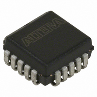
... Package (Note N.C. N. VCC 2 22 N.C. N. N.C. N. N.C. N. N.C. N. N. 32-Pin TQFP EPC1441 EPC1064 EPC1064V nCASC is a reserved pin and should N.C. VPP 23 N.C. 22 N.C. 21 N.C. 20 N.C. 19 N.C. 18 VPPSEL Altera Device Package Information © December 2009 Altera Corporation ...
Page 115
... April 2007 2.2 ■ July 2004 2.0 ■ September 2003 1.0 ■ © December 2009 Altera Corporation Package Temperature 32-pin TQFP 32-pin TQFP 20-pin PLCC 20-pin PLCC 20-pin PLCC 20-pin PLCC 8-pin PDIP 8-pin PDIP 32-pin TQFP 32-pin TQFP ...
Page 116
... Configuration Devices for SRAM-Based LUT Devices Data Sheet Configuration Handbook (Complete Two-Volume Set) Chapter Revision History © December 2009 Altera Corporation ...