EPC1213LC20 Altera, EPC1213LC20 Datasheet - Page 67
EPC1213LC20
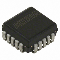
Manufacturer Part Number
EPC1213LC20
Description
IC CONFIG DEVICE 212KBIT 20-PLCC
Manufacturer
Altera
Series
EPCr
Datasheet
1.EPC4QI100N.pdf
(116 pages)
Specifications of EPC1213LC20
Programmable Type
OTP
Memory Size
212kb
Voltage - Supply
4.75 V ~ 5.25 V
Operating Temperature
0°C ~ 70°C
Package / Case
20-PLCC
For Use With
PLMJ1213 - PROGRAMMER ADAPTER 20 PIN J-LEAD
Lead Free Status / RoHS Status
Contains lead / RoHS non-compliant
Other names
544-2188-5
Available stocks
Company
Part Number
Manufacturer
Quantity
Price
Company:

Part Number:
EPC1213LC20
Manufacturer:
AT
Quantity:
23
Company:
Part Number:
EPC1213LC20
Manufacturer:
ALTERA
Quantity:
5 510
Company:
Part Number:
EPC1213LC20
Manufacturer:
TI
Quantity:
5 510
Part Number:
EPC1213LC20
Manufacturer:
ALTERA/阿尔特拉
Quantity:
20 000


Chapter 3: Serial Configuration Devices (EPCS1, EPCS4, EPCS16, EPCS64, and EPCS128) Data Sheet
Serial Configuration Device Memory Access
Table 3–8. Operation Codes for Serial Configuration Devices
© December 2009
Write enable
Write disable
Read status
Read bytes
Read silicon ID
Fast read
Write status
Write bytes
Erase bulk
Erase sector
Read Device
Identification
Notes to
(1) The MSB is listed first and the least significant bit (LSB) is listed last.
(2) The status register, data or silicon ID are read out at least once on the DATA pin and will continuously be read out until nCS is driven high.
(3) Write bytes operation requires at least one data byte on the DATA pin. If more than 256 bytes are sent to the device, only the last 256 bytes
(4) Read silicon ID operation is available only for EPCS1, EPCS4, EPCS16, and EPCS64.
(5) Read Device Identification operation is available only for EPCS128.
are written to the memory.
Operation
Table
(5)
3–8:
(4)
Altera Corporation
Write Enable Operation
The write enable operation code is b'0000 0110, and the MSB is listed first. The
write enable operation sets the write enable latch bit, which is bit 1 in the status
register. Always set the write enable latch bit before write bytes, write status, erase
bulk, and erase sector operations.
enable operation.
Figure 3–5. Write Enable Operation Timing Diagram
Operation Code
0000 0110
0000 0100
0000 0101
0000 0011
1010 1011
0000 1011
0000 0001
0000 0010
1100 0111
1101 1000
1001 1111
(1)
Figure 3–7
DCLK
DATA
ASDI
nCS
Address Bytes
0
0
0
3
0
3
0
3
0
3
0
and
High Impedance
Figure 3–8
Figure 3–5
0
1
Dummy Bytes
2
Operation Code
3
0
0
0
0
3
1
0
0
0
0
2
show the status register bit definitions.
shows the timing diagram for the write
4
Configuration Handbook (Complete Two-Volume Set)
5
6
7
1 to infinite
1 to infinite
1 to infinite
1 to infinite
1 to infinite
1 to 256
Data Bytes
0
0
1
0
0
(3)
(2)
(2)
(2)
(2)
(2)
DCLK f
(MHz)
25
25
25
20
25
40
25
25
25
25
25
MAX
3–15
Related parts for EPC1213LC20
Image
Part Number
Description
Manufacturer
Datasheet
Request
R

Part Number:
Description:
CUSTOMER ADVISORY EPC1064 and EPC1213 Transition Schedule Update
Manufacturer:
Altera Corporation
Part Number:
Description:
Configuration EPROMs For Flex Devices
Manufacturer:
Altera Corporation
Datasheet:

Part Number:
Description:
CYCLONE II STARTER KIT EP2C20N
Manufacturer:
Altera
Datasheet:

Part Number:
Description:
CPLD, EP610 Family, ECMOS Process, 300 Gates, 16 Macro Cells, 16 Reg., 16 User I/Os, 5V Supply, 35 Speed Grade, 24DIP
Manufacturer:
Altera Corporation
Datasheet:
Part Number:
Description:
CPLD, EP610 Family, ECMOS Process, 300 Gates, 16 Macro Cells, 16 Reg., 16 User I/Os, 5V Supply, 15 Speed Grade, 24DIP
Manufacturer:
Altera Corporation
Datasheet:
Part Number:
Description:
Manufacturer:
Altera Corporation
Datasheet:
Part Number:
Description:
CPLD, EP610 Family, ECMOS Process, 300 Gates, 16 Macro Cells, 16 Reg., 16 User I/Os, 5V Supply, 30 Speed Grade, 24DIP
Manufacturer:
Altera Corporation
Datasheet:
Part Number:
Description:
High-performance, low-power erasable programmable logic devices with 8 macrocells, 10ns
Manufacturer:
Altera Corporation
Datasheet:
Part Number:
Description:
High-performance, low-power erasable programmable logic devices with 8 macrocells, 7ns
Manufacturer:
Altera Corporation
Datasheet:
Part Number:
Description:
Classic EPLD
Manufacturer:
Altera Corporation
Datasheet:
Part Number:
Description:
High-performance, low-power erasable programmable logic devices with 8 macrocells, 10ns
Manufacturer:
Altera Corporation
Datasheet:
Part Number:
Description:
Manufacturer:
Altera Corporation
Datasheet:
Part Number:
Description:
Manufacturer:
Altera Corporation
Datasheet: