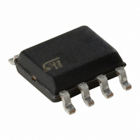
L6565D STMicroelectronics, L6565D Datasheet - Page 2

L6565D
Manufacturer Part Number
L6565D
Description
IC CTCLR PWM SMPS CM UVLO 8SOIC
Manufacturer
STMicroelectronics
Datasheet
1.L6565DTR.pdf
(17 pages)
Specifications of L6565D
Mfg Application Notes
25W Converter Using the L6565 AppNote 30 W Adapter with PWM L6565 Controller AppNote 80 W SMPS - L6565/ESBT STC04IE170HV AppNote L6565 Quasi-Resonant Controller AppNote L6565-Based Low Cost SMPS for TV AppNote SMPS for CRT Monitors with the L6565 AppNote STEVAL-TSP001V1 AppNote Wide Input Volt Range SMPS for Metering AppNote
Output Isolation
Isolated
Voltage - Input
10.3 ~ 18 V
Power (watts)
650mW
Operating Temperature
-40°C ~ 150°C
Package / Case
8-SOIC (0.154", 3.90mm Width)
Operating Temperature Range
- 40 C to + 150 C
Mounting Style
SMD/SMT
Input Voltage
12V
Output Current
200mA
Power Dissipation Pd
650mW
Digital Ic Case Style
SOIC
No. Of Pins
8
Rohs Compliant
Yes
For Use With
497-9051 - BOARD DEMO STC03DE220HV/ L6565497-8227 - BOARD EVAL L6565/STW3N150497-6427 - BOARD EVAL POE STHS4257A/L6565D497-6422 - BOARD EVAL BASED ON L6565497-6415 - BOARD EVAL L6565/STW4N150 BASED497-6414 - BOARD EVAL L6565 EU220V BASED497-6339 - BOARD EVAL SMPS L6565 3PHASE APP497-6255 - BOARD 6W 3PH SMPS METERING ESBT497-5680 - POWER SUPPLY FOR STB US-110V497-5679 - BOARD EVAL 3PHASE W/ESBT 100W
Lead Free Status / RoHS Status
Lead free / RoHS Compliant
Available stocks
Company
Part Number
Manufacturer
Quantity
Price
Part Number:
L6565D
Manufacturer:
ST
Quantity:
20 000
Part Number:
L6565D013TR
Manufacturer:
ST
Quantity:
20 000
Part Number:
L6565DTR
Manufacturer:
ST
Quantity:
20 000
L6565
DESCRIPTION (continued)
Converter's power capability variations with the mains voltage are compensated by line voltage feedforward.
At light load the device features a special function that automatically lowers the operating frequency still main-
taining the operation as close to ZVS as possible. In addition to very low start-up and quiescent currents, this
feature helps keep low the consumption from the mains at light load and be Blue Angel and Energy Star com-
pliant.
The IC includes also a disable function, an on-chip filter on current sense, an error amplifier with a precise ref-
erence voltage for primary regulation and an effective two-level overcurrent protection.
PIN CONNECTION (Top view, Minidip and SO8)
PIN DESCRIPTION
2/17
N°
1
2
3
4
5
6
7
8
COMP
Name
GND
ZCD
VFF
INV
Vcc
GD
CS
Inverting input of the error amplifier. The information on the output voltage is fed into the pin
through either a resistor divider (primary regulation) or an optocoupler (secondary feedback).
This pin can be grounded in some secondary feedback schemes (see pin 2).
Output of the error amplifier. Typically, a compensation network is placed between this pin and
the INV pin to achieve stability and good dynamic performance of the voltage control loop. With
secondary feedback, the pin can be also driven directly by an optocoupler to control PWM by
modulating the current sunk from the pin (with the INV pin grounded).
Line voltage feedforward. The information on the converter’s input voltage is fed into the pin
through a resistor divider and is used to change the setpoint of the pulse-by-pulse current
limitation (the higher the voltage, the lower the setpoint). If this function is not desired the pin will
be grounded and the current limitation setpoint will be maximum.
Input to the PWM comparator. The primary current is sensed through a resistor, the resulting
voltage is applied to this pin and compared with an internal reference to determine MOSFET’s
turn-off. The internal reference is clamped at a value, which defines the pulse-by-pulse current
limitation setpoint, depending on the voltage at pin VFF. If the signal at the pin CS exceeds 2 V,
the gate driver will be disabled (Hiccup-mode OCP).
Transformer’s demagnetization sensing input for Quasi-Resonant operation. Alternately,
synchronization input for an external signal. A negative-going edge triggers MOSFET’s turn-on.
The trigger circuit is blanked for a minimum of 3.5 µs after MOSFET turn-off, for safe operation
under short circuit conditions and frequency foldback. If the pin is grounded the IC will be
disabled.
Ground. Current return for both the signal part of the IC and the gate driver.
Gate driver output. The totem pole output stage is able to drive power MOSFET’s and IGBT’s
with a peak current of 400 mA (source and sink).
Supply Voltage of both the signal part of the IC and the gate driver. An electrolytic capacitor is
connected between this pin and ground. A resistor connected from this pin to the converter’s
input bulk capacitor will be typically used to start up the device.
COMP
VFF
INV
CS
1
2
3
4
Function
8
7
6
5
GND
Vcc
GD
ZCD


