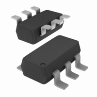
NCP1215ASNT1G ON Semiconductor, NCP1215ASNT1G Datasheet

NCP1215ASNT1G
Specifications of NCP1215ASNT1G
NCP1215ASNT1GOSTR
Related parts for NCP1215ASNT1G
NCP1215ASNT1G Summary of contents
Page 1
NCP1215A Low Cost Variable OFF Time Switched Mode Power Supply Controller The NCP1215A is a controller for low power off- -line flyback Switched Mode Power Supplies (SMPS) featuring low size, weight and cost constraints together with a good low standby ...
Page 2
Line Line + your application requires a gate--source resistor, please refer to design guidelines in this document. Feedback Loop FB Control -- V offset + 0-- 12.5--50 mA Current Sense Comparator + ...
Page 3
... ORDERING INFORMATION Device NCP1215ADR2G NCP1215ASNT1G †For information on tape and reel specifications, including part orientation and tape sizes, please refer to our Tape and Reel Packaging Specifications Brochure, BRD8011/D. Description The FB pin provides voltage feedback loop. The current injected into the pin determines the primary switch OFF time interval ...
Page 4
ELECTRICAL CHARACTERISTICS otherwise noted.) Characteristic VOLTAGE FEEDBACK Offset Voltage Maximum CT Pin Voltage at FB Current = 25 mA (Including V Maximum CT Pin Voltage at FB Current = 50 mA (Including V CT PIN - - OFF TIME CONTROL ...
Page 5
T , JUNCTION TEMPERATURE (C) J Figure 3. V Threshold vs. Junction startup Temperature 0.990 0.985 0.980 0.975 0.970 0.965 0.960 -- JUNCTION TEMPERATURE ...
Page 6
T , JUNCTION TEMPERATURE (C) J Figure 9. CT Pin Source Current vs. Junction Temperature 120 100 R source sink -- ...
Page 7
The NCP1215A implements a current mode SMPS with a variable OFF time dependant upon output power demand. It can be seen from the typical application that NCP1215A is designed to operate with a minimum number of external component. The NCP1215A ...
Page 8
To Current Sense Comparator Current 37.5 m Mirror 4:3 Figure 15. Feedback Loop - - Current Sense Control The resulting current sense regulation characteristic can be seen from Figure 16 12 ...
Page 9
Primary Current Sensing The primary current sensing circuit is shown in Figure 19. FB Feedback Loop 12.5 mA ÷ GND shift shift Figure 19. Primary Current Sensing When the ...
Page 10
If the IC current consumption is assumed constant during the startup phase, one can obtain resulting equation for startup resistor calculation: V bulk R startup = V startup C Vcc + I CC--start t startup Switching Frequency The switching frequency ...
Page 11
The EF16 core for transformer was selected. It has 2 cross- -section area The N67 magnetic e allows to use maximum operating B = 0.28 Tesla. max The number of turns of the primary winding ...
Page 12
Line S250 2 2.2 mF/ 2.2 mF/ Neutral 400 V 400 V IC1 ...
Page 13
Figure 24 shows CT voltage and also by Channel 2 the switch’s drain voltage at light load conditions. Figure 24. CT and Drain at Light Load The waveform on the current sense pin at full load conditions can be observed ...
Page 14
... S B 0.25 (0.010 - SEATING PLANE - - 0.25 (0.010 *For additional information on our Pb--Free strategy and soldering details, please download the ON Semiconductor Soldering and Mounting Techniques Reference Manual, SOLDERRM/D. PACKAGE DIMENSIONS SOIC SUFFIX CASE 751--07 ISSUE 0.10 (0.004 SOLDERING FOOTPRINT* 1.52 0.060 7.0 4.0 ...
Page 15
... A 0.05 A1 *For additional information on our Pb--Free strategy and soldering details, please download the ON Semiconductor Soldering and Mounting Techniques Reference Manual, SOLDERRM/D. ON Semiconductor and are registered trademarks of Semiconductor Components Industries, LLC (SCILLC). SCILLC reserves the right to make changes without further notice to any products herein. SCILLC makes no warranty, representation or guarantee regarding the suitability of its products for any particular purpose, nor does SCILLC assume any liability arising out of the application or use of any product or circuit, and specifically disclaims any and all liability, including without limitation special, consequential or incidental damages. “ ...


