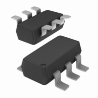
NCP1215ASNT1G ON Semiconductor, NCP1215ASNT1G Datasheet - Page 8

NCP1215ASNT1G
Manufacturer Part Number
NCP1215ASNT1G
Description
IC CTRLR CM UVLO 6TSOP
Manufacturer
ON Semiconductor
Datasheet
1.NCP1215ASNT1.pdf
(15 pages)
Specifications of NCP1215ASNT1G
Output Isolation
Isolated
Voltage - Input
8 ~ 18 V
Operating Temperature
25°C ~ 150°C
Package / Case
SC-74, SOT-457
Mounting Style
SMD/SMT
Lead Free Status / RoHS Status
Lead free / RoHS Compliant
Other names
NCP1215ASNT1G
NCP1215ASNT1GOSTR
NCP1215ASNT1GOSTR
12.5 mA
be seen from Figure 16.
decreases the peak current. This has the effect of slightly
increasing the switching frequency but the compression
ratio is selected to not hamper the standby power.
OFF Time Control
via an external capacitor, controls the switch- -off time. This
is portrayed in Figure 17.
FB
50 mA
Figure 16. Current Sense Regulation Characteristic
Figure 15. Feedback Loop - - Current Sense Control
The resulting current sense regulation characteristic can
When the load goes light, the compression circuitry
The loop signal together with the internal current source,
0 mA
To Current Sense Comparator
17 k
Current
Mirror
4:3
FB Pin Sink Current
50 mA
37.5 m
A
100 mA
12.5 m
A
http://onsemi.com
140 mA
CS
8
discharged by a MOSFET switch. As soon as the latch
output changes to a low state, the voltage across CT created
by the internal current source, starts to ramp- -up until its
value reaches the threshold given by the feedback loop
demand.
Figure 18. The bold waveform shows the maximum output
power when the OFF time is at its minimum. The IC allows
an OFF time of several seconds.
CT
During the switch- -ON time, the CT capacitor is kept
The voltage that can be observed on CT pin is shown in
Figure 18. CT Pin Voltage (P
Voltage
CT Pin
V
CT
offset
V
DD
V
Figure 17. OFF Time Control
10 mA
P
P
out
out
From Feedback Loop Block
t
Goes Down
Goes Up
off--min
V
offset
P1
P2
--
+
GND
P3
out1
+
--
> P
To Latch’s Set Input
To Latch’s Output
V
offset
out2
to V
> P
DD
out3
)
t


