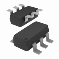
NCP1215ASNT1G ON Semiconductor, NCP1215ASNT1G Datasheet - Page 10

NCP1215ASNT1G
Manufacturer Part Number
NCP1215ASNT1G
Description
IC CTRLR CM UVLO 6TSOP
Manufacturer
ON Semiconductor
Datasheet
1.NCP1215ASNT1.pdf
(15 pages)
Specifications of NCP1215ASNT1G
Output Isolation
Isolated
Voltage - Input
8 ~ 18 V
Operating Temperature
25°C ~ 150°C
Package / Case
SC-74, SOT-457
Mounting Style
SMD/SMT
Lead Free Status / RoHS Status
Lead free / RoHS Compliant
Other names
NCP1215ASNT1G
NCP1215ASNT1GOSTR
NCP1215ASNT1GOSTR
the startup phase, one can obtain resulting equation for
startup resistor calculation:
Switching Frequency
input voltage. The highest frequency appears at highest
input voltage and maximum output power.
portion of the switching period can be calculated:
switch- -on time is:
voltage:
time linearly depends on the input bulk capacitor voltage.
Since this voltage has ripple due to AC input voltage and
input rectifier, it allows natural frequency dithering to
improve EMI signature of the SMPS.
external capacitor connected to the CT pin. The minimum
t
by:
decreases because the switch- -off time prolongs upon
feedback loop. The range of the frequency change is
sufficient to keep output voltage regulation in any light load
condition.
f sw-- max =
off
If the IC current consumption is assumed constant during
The switching frequency varies with the output load and
Since the peak primary current is fixed, the on time
Where:
L
I
Using equation for peak primary current estimation the
Minimum switch- -on time occurs at maximum input
As it can be seen from the above equation, the switch- -on
The switch- -off time is determined by the charge of an
Where:
V
I
The maximum switching frequency then can be evaluated
As output power diminishes, the switching frequency
pk
CT
value can be computed by:
p
offset
t on-- min = L p
Transformer primary inductance
Peak primary current
R startup =
=
t off-- min = C T
Offset voltage (see spec.)
CT pin source current (see spec.)
t on-- min + t off-- min
V bulk · R cs
t on = L p
L p · R shift
= 0.12 · 10 6 C T
t on = L p
C Vcc
· 50 · 10 --6 + 0.12 · 10 6 · C T
1
R cs · V bulk-- max
R cs · V bulk
R shift
V offset
V startup
t startup
R shift
I CT
1
V bulk
V bulk
I pk
+ I CC--start
= C T 1.2
50 · 10 --6
50 · 10 --6
10 --5
(eq. 10)
http://onsemi.com
(eq. 5)
(eq. 6)
(eq. 7)
(eq. 8)
(eq. 9)
10
Application Design Example
described hereafter.
wide range of the input voltage from 90 VAC up to 265 VAC.
The bulk capacitor voltage then can be calculated:
voltage is:
rated MOSFET switch is:
can be calculated:
input voltage is 75 kHz.
input voltage and its value can be estimated as follows:
operating frequency can be exploited for further calculation
of the primary inductance:
An example of the typical wall adapter application is
As a wall adapter it should be able to operate properly with
The requested output power is 5.2 Watts.
Assuming 80% efficiency the input power is equal to:
The average value of input current at minimum input
The suitable reflected primary winding voltage for 600 V
Using calculated flyback voltage the maximum duty cycle
Following equation determines peak primary current:
The desired maximum switching frequency at minimum
The highest switching frequency occurs at the highest
This frequency is much below 150 kHz, so that the desired
V bulk-- max = V AC-- max 2
V bulk-- min = V AC-- min 2
f max --high = f max --low
I in--avg =
V flbk = 600 V − V bulk-- max − V spike
I ppk =
δ max =
L p =
=
= 600 − 375 − 100 = 125 V
P in =
= 204.7 mA
=
V bulk-- min · δ max
0.2047 · 75 · 10 3
= 75 · 10 3 375
2 · I in--avg
V bulk-- min
I ppk · f sw-- max
V flbk + V bulk-- min
125 + 127
δ max
127 · 0.5
P out
P in
η =
125
V flbk
= 90 · 2
= 265 · 2
=
127
5.2
0.8
= 6.5
= 0.496 = 0.5
V bulk-- max
2 · 51.2 · 10 --3
V bulk-- min
127
= 6.5 W
0.5 = 110.7 kHz
= 4.14 mH
= 51.2 mA
0.5
= 127 VDC
= 375 VDC
δ max
(eq. 12)
(eq. 13)
(eq. 14)
(eq. 15)
(eq. 16)
(eq. 17)
(eq. 18)
(eq. 19)
(eq. 11)


