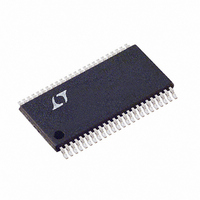
LTC1760CFW#PBF Linear Technology, LTC1760CFW#PBF Datasheet - Page 9

LTC1760CFW#PBF
Manufacturer Part Number
LTC1760CFW#PBF
Description
IC MANAGER BATTERY DUAL 48TSSOP
Manufacturer
Linear Technology
Datasheet
1.LTC1760CFWPBF.pdf
(44 pages)
Specifications of LTC1760CFW#PBF
Function
Charge Management
Battery Type
Smart Batteries
Voltage - Supply
6 V ~ 28 V
Operating Temperature
0°C ~ 70°C
Mounting Type
Surface Mount
Package / Case
48-TFSOP (0.240", 6.10mm Width)
Lead Free Status / RoHS Status
Lead free / RoHS Compliant
Available stocks
Company
Part Number
Manufacturer
Quantity
Price
PI FU CTIO S
GB2O (Pin 10): BAT2 Output Switch Gate Drive. Together
with GB2I, this pin drives the gate of the P-channel switch
in series with the BAT2 input switch.
GB2I (Pin 11): BAT2 Input Switch Gate Drive. Together
with GB2O, this pin drives the gate of the P-channel switch
connected to the BAT2 input.
CLP (Pin 36): This is the Positive Input to the Supply
Current Limiting Amplifier CL1. The threshold is set at
100mV above the voltage at the DCIN pin. When used to
limit supply current, a filter is needed to filter out the
switching noise.
Battery Charging Related
V
Divider which Provides Battery Voltage Feedback to the
Charger. A capacitor from CSN to V
to GND provide necessary compensation and filtering for
the voltage loop.
I
of the Current Mode PWM. Higher I
higher charging current in normal operation. A capacitor
of at least 0.1µF to GND filters out PWM ripple. Typical full-
scale output current is 30µA. Nominal voltage range for
this pin is 0V to 2.4V.
I
Filter Higher Frequency Components from the Delta-Sigma
IDAC.
I
between this pin and GND. The value of the external
resistor programs the range and resolution of the pro-
grammed charger current.
V
between this pin and GND. The value of the external
resistor programs the range and resolution of the voltage
DAC.
CSN (Pin 34): Current Amplifier CA1 Input. Connect this to
the common output of the charger MUX switches.
CSP (Pin 35): Current Amplifier CA1 Input. This pin and
the CSN pin measure the voltage across the sense resistor,
R
quired for both peak and average current mode operation.
TH
SET
LIMIT
SET
LIMIT
SENSE
U
(Pin 14): This is the Control Signal of the Inner Loop
(Pin 15): A Capacitor from I
(Pin 13): The Tap Point of a Programmable Resistor
(Pin 32): An external resistor (R
(Pin 33): An external resistor (R
, to provide the instantaneous current signals re-
U
U
SET
SET
to GND is Required to
ILIMIT
VLIMIT
TH
and one from V
corresponds to
) is connected
)is connected
SET
COMP1 (Pin 37): This is the Compensation Node for the
Amplifier CL1. A capacitor is required from this pin to
GND if input current amplifier CL1 is used. At input
adapter current limit, this node rises to 1V. By forcing
COMP1 to GND, amplifier CL1 will be defeated (no
adapter current limit). COMP1 can source 10µA.
BGATE (Pin 39): Drives the Gate of the Bottom External
MOSFET of the Battery Charger Buck Converter.
SW (Pin 42): Connected to Source of Top External MOSFET
Switch. Used as reference for top gate driver.
BOOST (Pin 43): Supply to Topside Floating Driver. The
bootstrap capacitor is returned to this pin. Voltage swing
at this pin is from a diode drop below V
TGATE (Pin 44): Drives the Gate of the Top External
MOSFET of the Battery Charger Buck Converter.
SCH1 (Pin 45), SCH2 (Pin 48): Charger MUX Switch
Source Returns. These two pins are connected to the
sources of Q3/Q4 and Q9/Q10 (see Typical Applications).
A small pull-down current source returns these nodes to
0V when the switches are turned off.
GCH1 (Pin 46), GCH2 (Pin 47): Charger MUX Switch
Gate Drives. These two pins drive the gates of the back-
to-back N-channel switch pairs, Q3/Q4 and Q9/Q10,
between the charger output and the two batteries (see
Typical Applications).
External Power Supply Pins
V
four internal diodes to the DCIN, SCN, BAT1, and BAT2
pins. Bypass this pin with a 0.1µF capacitor and a 1µF
capacitor. See Typical Applications for complete circuit.
BAT1 (Pin 3), BAT2 (Pin 2): These two pins are the inputs
from the two batteries for power to the LTC1760.
LOPWR (Pin 12): LOPWR Comparator Input from Exter-
nal Resistor Divider Connected from SCN to GND. If the
voltage at LOPWR pin is lower than the LOPWR com-
parator threshold, then system power has failed and
power is autonomously switched to a higher voltage
source, if available.
PLUS
(Pin 1): Supply. The V
PLUS
pin is connected via
CC
LTC1760
to (DCIN + V
CC
9
1760f
).


