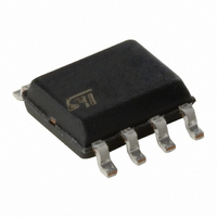
TSM1051CD STMicroelectronics, TSM1051CD Datasheet - Page 8

TSM1051CD
Manufacturer Part Number
TSM1051CD
Description
IC CONTROLLER CC/CV SMPS 8SOIC
Manufacturer
STMicroelectronics
Datasheet
1.TSM1051CD.pdf
(15 pages)
Specifications of TSM1051CD
Function
Charge Management
Battery Type
All Battery Types
Voltage - Supply
2.5 V ~ 12 V
Operating Temperature
0°C ~ 85°C
Mounting Type
Surface Mount
Package / Case
8-SOIC (0.154", 3.90mm Width)
Operating Supply Voltage
2.5 V to 12 V
Maximum Operating Temperature
+ 85 C
Minimum Operating Temperature
0 C
Mounting Style
SMD/SMT
Lead Free Status / RoHS Status
Contains lead / RoHS non-compliant
Other names
497-4478-5
Application information
5
5.1
5.1.1
5.1.2
8/15
Application information
Voltage and current control
Voltage control
The voltage loop is controlled via a first transconductance operational amplifier, the voltage
divider R
choose the values of R1 and R2 resistors using Equation 1.
where Vout is the desired output voltage.
To avoid the discharge of the load, the voltage divider R
this type of application, it is suggested a total value of 100 kΩ (or more) for resistors R1 and
R2
As an example, with R
Please note that if a low drop diode is inserted between the load and the voltage divider of
the voltage control loop in order to avoid current flowing from the load through the voltage
divider, the diode voltage drop should be taken into account in the computation of Equation
1 replacing V
Current control
The current loop is controlled via the second trans-conductance operational amplifier, the
sense resistor Rsense, and the optocoupler.
The control equation verifies:
where Ilim is the desired limited current, and Vsense is the threshold voltage for the current
control loop. As an example, with Ilim = 1 A, Vsense = -200 mV, then Rsense = 200 mΩ.
Note that the Rsense resistor should be chosen taking into account the maximum
dissipation (Plim) through it during full load operation.
As an example, with Ilim = 1 A, and Vsense = 200 mV, Plim = 200 mW.
Therefore, for most adaptor and battery charger applications, a quarter-watt, or half-watt
resistor to make the current sensing function is sufficient. Vsense threshold is achieved
internally by a voltage divider tied to the Vref voltage reference. Its middle point is tied to the
positive input of the current control operational amplifier, and its foot is to be connected to
lower potential point of the sense resistor as shown in
divider are matched to provide the best precision possible. The current sinking outputs of
the two trans-conductance operational amplifiers are common (to the output of the IC). This
makes an ORing function which ensures that whenever the current or the voltage reaches
too high values, the optocoupler is activated. The relation between the controlled current
and the controlled output voltage can be described with a square characteristic as shown in
the following V/I output-power graph. (with power supply of the device indipendent from the
output voltage)
1
Rsense x Ilim = Vsense
Rsense = Vsense / Ilim
Plim = Vsense x Ilim.
, R
2
out
, and the optocoupler which is directly connected to the output. Its possible to
with V
out
2
= 33 kΩ, V
+ V
R
drop
1
=
.
R
OUT
2
⋅
(
---------------------------------------
= 5 V, V
V
OUT
V
REF
–
Eq:3
Eq:2
Eq:2a
V
REF
REF
= 1.210 V, then R
)
Figure 3.
1
, R
Eq:1
2
should be highly resistive. For
The resistors of this voltage
1
= 103.4 kΩ
TSM1051


