NIS5135MN1TXG ON Semiconductor, NIS5135MN1TXG Datasheet - Page 2
NIS5135MN1TXG
Manufacturer Part Number
NIS5135MN1TXG
Description
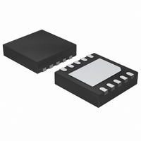
IC ELECTRONIC FUSE 10DFN
Manufacturer
ON Semiconductor
Datasheet
1.NIS5135MN1TXG.pdf
(11 pages)
Specifications of NIS5135MN1TXG
Function
Electronic Fuse
Voltage - Input
3.1 ~ 18 V
Current - Output
3.6A
Operating Temperature
-40°C ~ 150°C
Mounting Type
Surface Mount
Package / Case
10-VFDFN Exposed Pad
Polarity
Positive
Input Voltage Max
6.65 V
Maximum Operating Temperature
+ 150 C
Mounting Style
SMD/SMT
Linear Misc Type
Positive Voltage
Package Type
DFN EP
Operating Supply Voltage (min)
3.1V
Operating Supply Voltage (max)
18V
Operating Temperature (min)
-40C
Operating Temperature Classification
Automotive
Product Depth (mm)
3mm
Product Length (mm)
3mm
Mounting
Surface Mount
Pin Count
10
Lead Free Status / RoHS Status
Lead free / RoHS Compliant
Accuracy
-
Sensing Method
-
Lead Free Status / Rohs Status
Lead free / RoHS Compliant
Available stocks
Company
Part Number
Manufacturer
Quantity
Price

Part Number:
NIS5135MN1TXG
Manufacturer:
ON/安森美
Quantity:
20 000


Stresses exceeding Maximum Ratings may damage the device. Maximum Ratings are stress ratings only. Functional operation above the
Recommended Operating Conditions is not implied. Extended exposure to stresses above the Recommended Operating Conditions may affect
device reliability.
1. Negative voltage will not damage device provided that the power dissipation is limited to the rated allowable power for the package.
2. 1 oz copper, double−sided FR4.
3. Thermal limit is set above the maximum thermal rating. It is not recommended to operate this device at temperatures greater than the
Table 1. FUNCTIONAL PIN DESCRIPTION
MAXIMUM RATINGS
Input Voltage, operating, steady−state (V
Transient (100 ms)
Thermal Resistance, Junction−to−Air
Thermal Resistance, Junction−to−Lead (Pin 1)
Thermal Resistance, Junction−to−Case
Total Power Dissipation @ T
Derate above 25°C
Operating Temperature Range (Note 3)
Nonoperating Temperature Range
Lead Temperature, Soldering (10 Sec)
11 (belly pad)
maximum ratings for extended periods of time.
1−5
Pin
10
7
8
9
0.1 in
0.5 in
2
2
copper (Note 2)
copper (Note 2)
Enable/Fault
ENABLE/
Function
Ground
Source
FAULT
dv/dt
I
V
Limit
CC
A
= 25°C
Rating
Shutdown
Thermal
Enable
UVLO
This pin is the source of the internal power FET and the output terminal of the fuse.
A resistor between this pin and the source pin sets the overload and short circuit current limit
levels.
The enable/fault pin is a tri−state, bidirectional interface. It can be used to enable or disable the
output of the device by pulling it to ground using an open drain or open collector device. If a
thermal fault occurs, the voltage on this pin will go to an intermediate state to signal a monitoring
circuit that the device is in thermal shutdown. It can also be connected to another device in this
family to cause a simultaneous shutdown during thermal events.
The internal dv/dt circuit controls the slew rate of the output voltage at turn on. It has an internal
capacitor that allows it to ramp up over a period of 2 ms. An external capacitor can be added to
this pin to increase the ramp time. If an additional time delay is not required, this pin should be left
open.
Negative input voltage to the device. This is used as the internal reference for the IC.
Positive input voltage to the device.
CC
to GND, Note 1)
Figure 1. Block Diagram
http://onsemi.com
Charge
Pump
Voltage
Clamp
2
Current
Limit
VCC
Control
dv/dt
Description
Symbol
P
V
q
q
q
T
T
T
max
JA
JC
JL
IN
L
J
J
GND
SOURCE
I
dv/dt
LIMIT
−40 to 150
−55 to 155
−0.6 to 18
−0.6 to 25
Value
10.4
227
260
1.3
95
27
20
mW/°C
°C/W
°C/W
°C/W
Unit
°C
°C
°C
W
V
Related parts for NIS5135MN1TXG
Image
Part Number
Description
Manufacturer
Datasheet
Request
R

Part Number:
Description:
+5 Volt Electronic Fuse
Manufacturer:
ON Semiconductor
Datasheet:
Part Number:
Description:
ON Semiconductor [VOLTAGE REGULATOR]
Manufacturer:
ON Semiconductor
Datasheet:
Part Number:
Description:
357-036-542-201 CARDEDGE 36POS DL .156 BLK LOPRO
Manufacturer:
ON Semiconductor
Datasheet:
Part Number:
Description:
357-036-542-201 CARDEDGE 36POS DL .156 BLK LOPRO
Manufacturer:
ON Semiconductor
Datasheet:
Part Number:
Description:
357-036-542-201 CARDEDGE 36POS DL .156 BLK LOPRO
Manufacturer:
ON Semiconductor
Datasheet:
Part Number:
Description:
357-036-542-201 CARDEDGE 36POS DL .156 BLK LOPRO
Manufacturer:
ON Semiconductor
Datasheet:
Part Number:
Description:
357-036-542-201 CARDEDGE 36POS DL .156 BLK LOPRO
Manufacturer:
ON Semiconductor
Datasheet:
Part Number:
Description:
357-036-542-201 CARDEDGE 36POS DL .156 BLK LOPRO
Manufacturer:
ON Semiconductor
Datasheet:
Part Number:
Description:
357-036-542-201 CARDEDGE 36POS DL .156 BLK LOPRO
Manufacturer:
ON Semiconductor
Datasheet:
Part Number:
Description:
357-036-542-201 CARDEDGE 36POS DL .156 BLK LOPRO
Manufacturer:
ON Semiconductor
Datasheet:
Part Number:
Description:
357-036-542-201 CARDEDGE 36POS DL .156 BLK LOPRO
Manufacturer:
ON Semiconductor
Datasheet:
Part Number:
Description:
357-036-542-201 CARDEDGE 36POS DL .156 BLK LOPRO
Manufacturer:
ON Semiconductor
Datasheet:
Part Number:
Description:
Manufacturer:
ON Semiconductor
Datasheet:
Part Number:
Description:
Manufacturer:
ON Semiconductor
Datasheet: