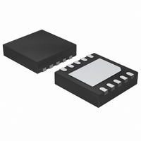
NIS5135MN1TXG ON Semiconductor, NIS5135MN1TXG Datasheet - Page 8

NIS5135MN1TXG
Manufacturer Part Number
NIS5135MN1TXG
Description
IC ELECTRONIC FUSE 10DFN
Manufacturer
ON Semiconductor
Datasheet
1.NIS5135MN1TXG.pdf
(11 pages)
Specifications of NIS5135MN1TXG
Function
Electronic Fuse
Voltage - Input
3.1 ~ 18 V
Current - Output
3.6A
Operating Temperature
-40°C ~ 150°C
Mounting Type
Surface Mount
Package / Case
10-VFDFN Exposed Pad
Polarity
Positive
Input Voltage Max
6.65 V
Maximum Operating Temperature
+ 150 C
Mounting Style
SMD/SMT
Linear Misc Type
Positive Voltage
Package Type
DFN EP
Operating Supply Voltage (min)
3.1V
Operating Supply Voltage (max)
18V
Operating Temperature (min)
-40C
Operating Temperature Classification
Automotive
Product Depth (mm)
3mm
Product Length (mm)
3mm
Mounting
Surface Mount
Pin Count
10
Lead Free Status / RoHS Status
Lead free / RoHS Compliant
Accuracy
-
Sensing Method
-
Lead Free Status / Rohs Status
Lead free / RoHS Compliant
Available stocks
Company
Part Number
Manufacturer
Quantity
Price
Part Number:
NIS5135MN1TXG
Manufacturer:
ON/安森美
Quantity:
20 000
Basic Operation
It contains circuits to monitor the input voltage, output
voltage, output current and die temperature.
the input voltage to the load based on the restrictions of the
controlling circuits. The dv/dt of the output voltage will be
controlled by the internal dv/dt circuit. The output voltage
will slew from 0 V to the rated output voltage in 2 ms, unless
additional capacitance is added to the dv/dt pin.
not exceed the 175°C limit that is programmed into the chip.
The current limit circuit does not shut down the part but will
reduce the conductivity of the FET to maintain a constant
current at the internally set current limit level. The input
overvoltage clamp also does not shutdown the part, but will
limit the output voltage to 6.65 V in the event that the input
exceeds that level.
of the internal n−channel power FET and also for the current
limit circuit. The remainder of the control circuitry operates
between the input voltage (V
Current Limit
reference and amplifier to control the peak current in the
device. The SENSEFET allows for a small fraction of the
load current to be measured, which has the advantage of
reducing the losses in the sense resistor as well as increasing
the value and decreasing the power rating of the sense
resistor. Sense resistors are typically in the tens of ohms
range with power ratings of several milliwatts making them
very inexpensive chip resistors.
short circuit events which are defined as the mode of
operation in which the gate is high and the FET is fully
enhanced. The overload mode of operation occurs when the
This device is a self−protected, resettable, electronic fuse.
On application of the input voltage, the device will apply
The device will remain on as long as the temperature does
An internal charge pump provides bias for the gate voltage
The current limit circuit uses a SENSEFET along with a
The current limit circuit has two limiting values, one for
CC
) and ground.
140
120
100
80
60
3.0
Figure 18. On Resistance vs. V
APPLICATION INFORMATION
http://onsemi.com
4.0
V
CC
8
(V)
device is actively limiting the current and the gate is at an
intermediate level. For a more detailed description of this
circuit please refer to application note AND8140.
for this device. They are shown in the two application
figures. Direct current sensing connects the sense resistor
between the current limit pin and the load. This method
includes the bond wire resistance in the current limit circuit.
This resistance has an impact on the current limit levels for
a given resistor and may vary slightly depending on the
impedance between the sense resistor and the source pins.
The on resistance of the device will be slightly lower in this
configuration since all five source pins are connected in
parallel and therefore, the effective bond wire resistance is
one fifth of the resistance for any given pin.
of the source pins as the connection for the current sense
resistor. This connection senses the voltage on the die and
therefore any bond wire resistance and external impedance
on the board have no effect on the current limit levels. In this
configuration the on resistance is slightly increased relative
to the direct sense method since only for of the source pins
are used for power.
Overvoltage Clamp
reference. It monitors the output voltage and if the input
voltage exceeds 6.65 V, the gate drive of the main FET is
reduced to limit the output. This is intended to allow
operation through transients while protecting the load. If an
overvoltage condition exists for many seconds, the device
may overheat due to the voltage drop across the FET
combined with the load current. In this event, the thermal
protection circuit would shut down the device.
There are two methods of biasing the current limit circuit
The other method is Kelvin sensing. This method uses one
The overvoltage clamp consists of an amplifier and
5.0
CC
6.0


