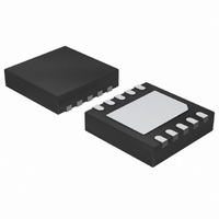
NIS5135MN1TXG ON Semiconductor, NIS5135MN1TXG Datasheet - Page 9

NIS5135MN1TXG
Manufacturer Part Number
NIS5135MN1TXG
Description
IC ELECTRONIC FUSE 10DFN
Manufacturer
ON Semiconductor
Datasheet
1.NIS5135MN1TXG.pdf
(11 pages)
Specifications of NIS5135MN1TXG
Function
Electronic Fuse
Voltage - Input
3.1 ~ 18 V
Current - Output
3.6A
Operating Temperature
-40°C ~ 150°C
Mounting Type
Surface Mount
Package / Case
10-VFDFN Exposed Pad
Polarity
Positive
Input Voltage Max
6.65 V
Maximum Operating Temperature
+ 150 C
Mounting Style
SMD/SMT
Linear Misc Type
Positive Voltage
Package Type
DFN EP
Operating Supply Voltage (min)
3.1V
Operating Supply Voltage (max)
18V
Operating Temperature (min)
-40C
Operating Temperature Classification
Automotive
Product Depth (mm)
3mm
Product Length (mm)
3mm
Mounting
Surface Mount
Pin Count
10
Lead Free Status / RoHS Status
Lead free / RoHS Compliant
Accuracy
-
Sensing Method
-
Lead Free Status / Rohs Status
Lead free / RoHS Compliant
Available stocks
Company
Part Number
Manufacturer
Quantity
Price
Part Number:
NIS5135MN1TXG
Manufacturer:
ON/安森美
Quantity:
20 000
Undervoltage Lockout
hysteresis to monitor the input voltage. If the input voltage
drops below the specified level, the output switch will be
switched to a high impedance state.
dv/dt Circuit
linear, controlled rate regardless of the load impedance
characteristics. An internal ramp generator creates a linear
ramp, and a control circuit forces the output voltage to
follow that ramp, scaled by a factor.
modified by adding an external capacitor at the dv/dt pin.
This pin includes an internal current source of
approximately 85 nA. Since the current level is very low, it
is important to use a ceramic cap or other low leakage
capacitor. Aluminum electrolytic capacitors are not
recommended for this circuit.
be determined by the following equation, where t is in
seconds:
Where:
C is in Farads
t is in Seconds
shut−down, or recycling of input power, the timing capacitor
will be discharged and the output voltage will ramp from 0
at turn on.
Enable/Fault
pin that can control the output of the chip as well as send
information to other devices regarding the state of the chip.
The undervoltage lockout circuit uses a comparator with
The dv/dt circuit brings the output voltage up under a
The default ramp time is approximately 2 ms. This can be
The ramp time from 0 to the nominal output voltage can
Any time that the unit shuts down due to a fault, enable
The Enable/Fault Pin is a multi−function, bidirectional
t
0−5
C
+ 30e6 @ (50 pF ) C
ext
+
30e6
t
0−5
* 50 pF
ext
Figure 19. Enable/Fault Signal Levels
)
http://onsemi.com
9
When this pin is low, the output of the fuse will be turned off.
When this pin is high the output of the fuse will be
turned−on. If a thermal fault occurs, this pin will be pulled
low to an intermediate level by an internal circuit.
collector device should be connected to this pin. Due to its
tri−state operation, it should not be connected to any type of
logic with an internal pullup device.
its thermal limit, this pin will be pulled down to an
intermediate level. This signal can be monitored by an
external circuit to communicate that a thermal shutdown has
occurred. If this pin is tied to another device in this family
(NIS5132 or NIS5135), a thermal shutdown of one device
will cause both devices to disable their outputs. Both devices
will turn on once the fault is removed for the auto−retry
devices.
enabled after the enable pin has been pulled to ground with
an external switch and then allowed to go high or after the
input power has been recycled. For the auto retry devices,
both devices will restart as soon as the die temperature of the
device in shutdown has been reduced to the lower thermal
limit. The thermal options are listed in the ordering table.
Thermal Protection
circuit that senses the temperature on the die of the power
FET. If the temperature reaches 175°C, the device will shut
down, and remove power from the load. Output power can
be restored by either recycling the input power or toggling
the enable pin. Power will automatically be reapplied to the
load for auto−retry devices once the die temperature has
been reduced by 45°C.
increase the trip time during high power transient events. It
is not recommended to operate this device above 150°C for
extended periods of time.
To use as a simple enable pin, an open drain or open
If the chip shuts down due to the die temperature reaching
For the latching thermal device, the outputs will be
The NIS5135 includes an internal temperature sensing
The thermal limit has been set high intentionally, to


