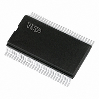
PCF8576CT/1,112 NXP Semiconductors, PCF8576CT/1,112 Datasheet - Page 23

PCF8576CT/1,112
Manufacturer Part Number
PCF8576CT/1,112
Description
IC LCD DVR UNVRSL LOW-MUX 56VSOP
Manufacturer
NXP Semiconductors
Specifications of PCF8576CT/1,112
Package / Case
56-VSOP
Display Type
LCD
Configuration
40 Segment
Interface
I²C
Current - Supply
120µA
Voltage - Supply
2 V ~ 6 V
Operating Temperature
-40°C ~ 85°C
Mounting Type
Surface Mount
Number Of Digits
20
Number Of Segments
160
Maximum Clock Frequency
315 KHz
Operating Supply Voltage
2 V to 6 V
Maximum Power Dissipation
400 mW
Maximum Operating Temperature
+ 85 C
Attached Touch Screen
No
Maximum Supply Current
120 uA
Minimum Operating Temperature
- 40 C
Lead Free Status / RoHS Status
Lead free / RoHS Compliant
Digits Or Characters
-
Lead Free Status / Rohs Status
Lead free / RoHS Compliant
Other names
935278818112
PCF8576CTD
PCF8576CTD
PCF8576CTD
PCF8576CTD
NXP Semiconductors
PCF8576C
Product data sheet
7.14.1 Output bank selector
7.14.2 Input bank selector
7.14 Bank selector
7.15 Blinker
The output bank selector (see
address for transfer to the display register. The actual row selected depends on the LCD
drive mode in operation and on the instant in the multiplex sequence.
The PCF8576C includes a RAM bank switching feature in the static and 1:2 multiplex
drive modes. In the static drive mode, the bank-select command may request the contents
of row 2 to be selected for display instead of the contents of row 0. In 1:2 multiplex drive
mode, the contents of rows 2 and 3 may be selected instead of rows 0 and 1. This
enables preparation of display information in an alternative bank and the ability to switch
to it once it has been assembled.
The input bank selector (see
the selected LCD drive configuration. Using the bank-select command, display data can
be loaded in row 2 into static drive mode or in rows 2 and 3 into 1:2 multiplex drive mode.
The input bank selector functions independently of the output bank selector.
The display blinking capabilities of the PCF8576C are very versatile. The whole display
can be blinked at frequencies selected by the blink-select command. The blinking
frequencies are integer fractions of the clock frequency; the ratios between the clock and
blinking frequencies depend on the mode in which the device is operating (see
Table 7.
An additional feature is for an arbitrary selection of LCD segments to be blinked. This
applies to the static and 1:2 multiplex drive modes and can be implemented without any
communication overheads. Using the output bank selector, the displayed RAM banks are
exchanged with alternate RAM banks at the blinking frequency. This mode can also be
specified by the blink-select command (see
Blinking mode
off
1
2
3
•
•
•
•
In 1:4 multiplex mode: all RAM addresses of row 0 are selected, followed sequentially
by the contents of row 1, row 2, and then row 3.
In 1:3 multiplex mode: rows 0, 1, and 2 are selected sequentially.
In 1:2 multiplex mode: rows 0 and 1 are selected.
In the static mode: row 0 is selected.
Blink frequencies
All information provided in this document is subject to legal disclaimers.
Normal-power mode
ratio
-
f
f
f
Rev. 10 — 22 July 2010
blink
blink
blink
=
=
=
Table
Table
--------------- -
92160
------------------- -
184320
------------------- -
368640
f
f
f
clk
clk
clk
12) loads display data into the display RAM based on
12), selects one of the four rows per display RAM
Universal LCD driver for low multiplex rates
Table
Power-saving mode
ratio
-
f
f
f
blink
blink
blink
13).
=
=
=
--------------- -
15360
--------------- -
30720
--------------- -
61440
f
f
f
clk
clk
clk
PCF8576C
Blink frequency
blinking off
2 Hz
1 Hz
0.5 Hz
© NXP B.V. 2010. All rights reserved.
Table
23 of 57
7).


