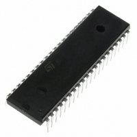
M5450B7 STMicroelectronics, M5450B7 Datasheet - Page 4

M5450B7
Manufacturer Part Number
M5450B7
Description
IC LED DISPLAY DRIVER 40-PDIP
Manufacturer
STMicroelectronics
Datasheet
1.M5450B7.pdf
(12 pages)
Specifications of M5450B7
Display Type
LED
Configuration
Alphanumeric or Dot Matrix
Interface
Serial
Digits Or Characters
4 or 5 Digits
Current - Supply
7mA
Voltage - Supply
4.75 V ~ 13.2 V
Operating Temperature
-25°C ~ 85°C
Mounting Type
Through Hole
Package / Case
40-DIP (0.600", 15.24mm)
Operating Supply Voltage (typ)
5/9/12V
Number Of Digits
5
Number Of Segments
34
Operating Temperature (min)
-25C
Operating Temperature (max)
85C
Operating Temperature Classification
Commercial
Package Type
PDIP
Pin Count
40
Mounting
Through Hole
Power Dissipation
1W
Operating Supply Voltage (min)
4.75V
Operating Supply Voltage (max)
13.2V
Low Level Output Current
25 mA
Operating Supply Voltage
4.75 V to 13.2 V
Maximum Supply Current
7 mA
Maximum Power Dissipation
1 W
Maximum Operating Temperature
+ 85 C
Mounting Style
Through Hole
Minimum Operating Temperature
- 25 C
Lead Free Status / RoHS Status
Lead free / RoHS Compliant
Available stocks
Company
Part Number
Manufacturer
Quantity
Price
Part Number:
M5450B7
Manufacturer:
ST
Quantity:
20 000
M5450, M5451
Table 2. Static Electrical Characteristics
Note: 1. Output matching is calculated as the percent variation from I
Figure 4. Input Data Format
4/12
(T
Symbol
amb
V
f
V
clock
I
O(off)
V
DD
V
I
I
I
2. With a fixed resistor on the brightness input some variation in brightness will occur from one device to another.
3. Absolute maximum for each output should be limited to 40mA.
4. The V
DD
O
O
B
B
I
within operating range, V
CLOCK
DATA
LOAD
(INTERNAL)
RESET
(INTERNAL)
O
Supply Voltage
Supply Current
Input Voltage Logical "0" Level
Logical "1" Level
Brightness Input Current (note 2)
Brightness Input Voltage (pin 19) Input Current = 750µA, T
Off State Out. Voltage
Out. Sink Current (note 3)
Segment OFF
Segment ON
Input Clock Frequency
Output Matching (note 1)
voltage should be regulated by the user. See Figure 7 and Figure 8 for allowable VO versus IO operation.
Parameter
START
1
DD
BIT 1
= 4.75V to 13.2V, V
V
± 10µA Input Bias
4.75 ≤ V
V
V
V
Brightness In. = 0µA
Brightness In. = 100µ
Brightness In. = 750µA
DD
DD
O
O
= 3V
= 1V (note 4)
= 13.2V
> 5.25
DD
Test Conditions
≤ 5.25
MAX
SS
+ I
= 0V, unless otherwise specified)
MIN
/2.
amb
= 25°C
BIT 34
V
BIT 35
Min.
4.75
- 0.3
2.2
DD
36
12
2
0
3
0
0
- 2
Typ.
15
27
13.2
Max.
0.75
0.5
± 20
13.2
0.8
V
4.3
V
10
10
25
7
DD
4
DD
MHz
Unit
V
mA
mA
mA
µA
µA
mA
%
V
V
V
V
V


