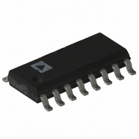
ADE7769AR Analog Devices Inc, ADE7769AR Datasheet - Page 12

ADE7769AR
Manufacturer Part Number
ADE7769AR
Description
IC ENERGY METER POS W/OSC 16SOIC
Manufacturer
Analog Devices Inc
Datasheet
1.ADE7769ARZ-RL.pdf
(20 pages)
Specifications of ADE7769AR
Input Impedance
320 KOhm
Measurement Error
0.1%
Voltage - I/o High
2.4V
Voltage - I/o Low
0.8V
Current - Supply
5mA
Voltage - Supply
4.75 V ~ 5.25 V
Operating Temperature
-40°C ~ 85°C
Mounting Type
Surface Mount
Package / Case
16-SOIC (0.154", 3.90mm Width)
Meter Type
Single Phase
Lead Free Status / RoHS Status
Contains lead / RoHS non-compliant
Available stocks
Company
Part Number
Manufacturer
Quantity
Price
Part Number:
ADE7769AR
Manufacturer:
ADI/亚德诺
Quantity:
20 000
Part Number:
ADE7769ARZ
Manufacturer:
ADI/亚德诺
Quantity:
20 000
ADE7769
POWER SUPPLY MONITOR
The ADE7769 contains an on-chip power supply monitor. The
power supply (V
If the supply is less than 4 V, the ADE7769 becomes inactive.
This is useful to ensure proper device operation at power-up
and power-down. The power supply monitor has built-in
hysteresis and filtering, which provide a high degree of
immunity to false triggering from noisy supplies.
In Figure 21, the trigger level is nominally set at 4 V. The toler-
ance on this trigger level is within ±5%. The power supply and
decoupling for the part should be such that the ripple at V
does not exceed 5 V ± 5%, as specified for normal operation.
HPF and Offset Effects
Figure 22 shows the effect of offsets on the real power calcula-
tion. As can be seen, offsets on Channel V1 and Channel V2
contribute a dc component after multiplication. Because this dc
component is extracted by the LPF and used to generate the real
power information, the offsets contribute a constant error to the
real power calculation. This problem is easily avoided by the
built-in HPF in Channel V1. By removing the offsets from at
least one channel, no error component can be generated at dc
by the multiplication. Error terms at the line frequency (ω) are
removed by the LPF and the digital-to-frequency conversion
(see the Digital-to-Frequency Conversion section).
ACTIVATION
INTERNAL
NEUTRAL
V
DD
5V
4V
0V
Figure 20. Typical Connections for Channel V2
Figure 21. On-Chip Power Supply Monitor
PHASE
INACTIVE
DD
R
) is continuously monitored by the ADE7769.
A
*
R
B
*R
A
R
>> R
ACTIVE
F
TIME
B
+ R
C
F
F
R
±165mV
F
INACTIVE
C
F
V2P
V2N
DD
Rev. A | Page 12 of 20
Equation 6 shows how the power calculation is affected by the
dc offsets in the current and voltage channels.
The HPF in Channel V1 has an associated phase response that
is compensated for on chip. Figure 23 and Figure 24 show the
phase error between channels with the compensation network
activated. The ADE7769 is phase compensated up to 1 kHz as
shown. This ensures correct active harmonic power calculation
even at low power factors.
=
+
Figure 22. Effect of Channel Offset on the Real Power Calculation
{
–0.05
–0.10
V
V
0.30
0.25
0.20
0.15
0.10
0.05
V
OS
V
V × I
cos
0
Figure 23. Phase Error Between Channels (0 Hz to 1 kHz)
2
2
×
× I
×
2
0
OS
I
I
( )
+
ωt
×
100
0
V
cos
OS
+
(
×
V
200
2
OS
I
ωt
OS
DC COMPONENT (INCLUDING ERROR TERM)
IS EXTRACTED BY THE LPF FOR REAL
POWER CALCULATION
}
)
300
×
+
{
V
I
V
I
FREQUENCY (RAD/s)
OS
OS
OS
FREQUENCY (Hz)
cos
400
× V
× I
×
( )
I
ωt
cos
500
+
( )
ωt
600
I
OS
+
}
700
I
OS
×
800
V
cos
900 1000
( )
ωt
(6)


