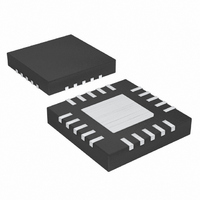
MAX3740AETG+T Maxim Integrated Products, MAX3740AETG+T Datasheet - Page 12

MAX3740AETG+T
Manufacturer Part Number
MAX3740AETG+T
Description
IC DRIVER SFP VCSEL 24-TQFN
Manufacturer
Maxim Integrated Products
Type
Laser Diode Driverr
Datasheet
1.MAX3740AETG.pdf
(15 pages)
Specifications of MAX3740AETG+T
Data Rate
3.2Gbps
Number Of Channels
1
Voltage - Supply
2.97 V ~ 3.63 V
Current - Supply
55mA
Current - Modulation
15mA
Current - Bias
15mA
Operating Temperature
-40°C ~ 85°C
Package / Case
24-TQFN Exposed Pad
Mounting Type
Surface Mount
Supply Voltage (max)
6 V
Maximum Operating Temperature
+ 85 C
Mounting Style
SMD/SMT
Minimum Operating Temperature
- 40 C
Supply Current
55 mA
Lead Free Status / RoHS Status
Lead free / RoHS Compliant
3.2Gbps SFP VCSEL Driver with Diagnostic
Monitors
The modulation current output of the MAX3740A is con-
trolled by a resistor (R
MODSET and ground. The R
the amount of current being sourced to the VCSEL. The
modulation current is given by the following:
It is important to note that the modulation current being
sourced by the MAX3740A is affected by the load
impedance of the VCSEL. The Modulation Current vs.
R
shows the current into a 50Ω electrical load.
The bias current output of the MAX3740A is controlled
by a resistor (R
ground. In open-loop operation the R
the bias current level of the VCSEL. In closed-loop
operation the R
rent provided by the APC. The bias current is given by
the following:
The Bias Current vs. R
the Typical Operating Characteristics .
To ensure stable operation of the APC circuit, the time
constant of the MD node should be shorter than the
APC time constant. (t
For typical I
photodiode with capacitance less than 500pF.
Compute the required modulation tempco from the
slope efficiency of the laser at T
higher temperature. Then select the value of R
the Typical Operating Characteristics . For example,
suppose a laser has a slope efficiency (SE) of
12
I
I
MOD
MOD
MODSET
Programming Modulation-Current Tempco
___________________________________________________
=
=
t MD
[
⎡
⎢
⎢
⎣
(
⎛
⎜
⎝
I
MODSET
graph in the Typical Operating Characteristics
200
I
I
≤
BIAS
BIAS
t APC
Programming Modulation Current
PD
20
+
BIASSET
BIASSET
=
=
R
= 400µA, R
(
,
1
MODSET
⎛
⎜
⎝
I
)
BIASSET
200
×
R
MD
30
APC
Programming Bias Current
+
]
) placed between BIASSET and
BIASSET
controls the maximum bias cur-
×
×
R
1 2
= 5µs if C
C
⎞
⎟ ×
⎠
.
BIASSET
⎡
⎢
⎣
MODSET
)
R
MD
×
Photodiode Selection
PWRSET
OUT
30
34
MODSET
≤
R
⎤
⎥
⎥
⎦
graph is also shown in
+
5
×
OUT
20
μ
⎞
⎟ ×
⎠
A
+
⎡
⎢
⎣
APC
s
) placed between
R
R
= +25°C and at a
=
+
OUT
34
= 500Ω, select a
LOAD
250
BIASSET
resistor controls
= 0.047µF).
R
+
OUT
ns
+
⎤
⎥
⎦
R
+
LOAD
controls
TC
from
⎤
⎥
⎦
0.021mW/mA at +25°C, which reduces to 0.018mW/mA
at +85°C. The temperature coefficient is given by the
following:
From the Typical Operating Characteristics , the value
of R
modulation temperature compensation is not desired,
short TC1 and TC2.
Program the average optical power by adjusting
R
desired monitor current to be maintained over tempera-
ture and lifetime. See the Monitor Diode Current vs.
R
section, and select the value of R
sponds to the required current.
The MAX3740A data inputs are SFP MSA compatible.
On-chip 100Ω differential input impedance is provided
for optimal termination (Figure 4). Because of the on-chip
biasing network, the MAX3740A inputs self-bias to the
proper operating point to accommodate AC-coupling.
Figure 4. Simplified Input Structure
Laser tempco
PWRSET
PWRSET
IN+
IN-
TC
PACKAGE
, which offsets the tempco of the laser, is 9kΩ. If
MAX3740A
1nH
1nH
graph in the Typical Operating Characteristics
. To select the resistance, determine the
0.5pF
0.5pF
Input Termination Requirements
= −
=
SE
(
2380
SE
25
Programming the APC Loop
85
V
V
×
ppm C
CC
CC
−
(
85 25
SE
50Ω
50Ω
/
−
°
25
16kΩ
24kΩ
)
)
×
1 6
E
PWRSET
V
CC
that corre-


