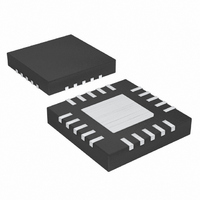
MAX3740AETG+T Maxim Integrated Products, MAX3740AETG+T Datasheet - Page 2

MAX3740AETG+T
Manufacturer Part Number
MAX3740AETG+T
Description
IC DRIVER SFP VCSEL 24-TQFN
Manufacturer
Maxim Integrated Products
Type
Laser Diode Driverr
Datasheet
1.MAX3740AETG.pdf
(15 pages)
Specifications of MAX3740AETG+T
Data Rate
3.2Gbps
Number Of Channels
1
Voltage - Supply
2.97 V ~ 3.63 V
Current - Supply
55mA
Current - Modulation
15mA
Current - Bias
15mA
Operating Temperature
-40°C ~ 85°C
Package / Case
24-TQFN Exposed Pad
Mounting Type
Surface Mount
Supply Voltage (max)
6 V
Maximum Operating Temperature
+ 85 C
Mounting Style
SMD/SMT
Minimum Operating Temperature
- 40 C
Supply Current
55 mA
Lead Free Status / RoHS Status
Lead free / RoHS Compliant
ABSOLUTE MAXIMUM RATINGS
Supply Voltage (V
Voltage at TX_DISABLE, IN+, IN-, FAULT,
Voltage at OUT+, OUT- .........................(V
Current into FAULT ............................................ -1mA to +25mA
Current into OUT+, OUT- ....................................................60mA
3.2Gbps SFP VCSEL Driver with Diagnostic
Monitors
ELECTRICAL CHARACTERISTICS
(V
+25°C, unless otherwise noted.)
Stresses beyond those listed under “Absolute Maximum Ratings” may cause permanent damage to the device. These are stress ratings only, and functional
operation of the device at these or any other conditions beyond those indicated in the operational sections of the specifications is not implied. Exposure to
absolute maximum rating conditions for extended periods may affect device reliability.
2
Supply Current
FAULT OUTPUT
Output High Voltage
Output Low Voltage
TX_DISABLE INPUT
Input Impedance
Input High Voltage
Input Low Voltage
Power-Down Time
SQUELCH
Squelch Threshold
Squelch Hysteresis
Time to Squelch Data
Time to Resume from Squelch
BIAS GENERATOR (Note 4)
Bias Current
Accuracy of Programmed Bias
Current
SQUELCH, TC1, TC2, MODSET, PEAKSET, BIASSET,
BIAS, BIASMON, COMP, MD, REF,
PWRMON ...............................................-0.5V to (V
CC
_______________________________________________________________________________________
= +2.97V to +3.63V, T
PARAMETER
CC
) ..............................................-0.5V to 6.0V
A
= -40°C to +85°C. Typical values are at V
SYMBOL
I
CC-SHDN
ΔBIAS
I
V
V
BIAS
I
V
CC
V
CC
OH
OL
IH
IL
- 2V) to (V
SQUELCH set low,
TX_DISABLE set low,
peaking is not used
(Note 1)
Additional current when peaking is used
(Note 2)
Additional current when SQUELCH is high
Total current when TX_DISABLE is high
R
R
The time for I
TX_DISABLE transitions high
(Note 3)
(Note 3)
Minimum
Maximum
5mA ≤ I
1mA ≤ I
LOAD
LOAD
CC
CC
+ 0.5V)
= 10kΩ to 2.97V
= 4.7kΩ to 3.63V
BIAS
BIAS
+ 2V)
≤ 15mA
≤ 5mA
CC
CONDITIONS
to reach I
Continuous Power Dissipation (T
Operating Temperature Range ...........................-40°C to +85°C
Storage Temperature Range .............................-55°C to +150°C
Lead Temperature (soldering, 10s) .................................+300°C
24-Lead Thin QFN
(derate 20.8mW/°C above +85°C).................................1354mW
CC
I
I
MOD
MOD
= +3.3V, TC1 and TC2 are shorted, PEAKSET open, T
CC-SHDN
= 2mA
= 15mA
when
P-P
P-P
0.02
0.02
MIN
2.4
4.7
2.0
-12
25
10
15
-8
A
= +85°C)
TYP
3.9
32
55
15
50
5
MAX
10.0
5.00
5.00
+12
0.4
0.8
+8
68
20
10
85
5
1
UNITS
mV
mV
mA
mA
kΩ
µs
µs
µs
%
V
V
V
V
P-P
P-P
A
=


