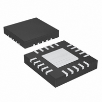
MAX3740AETG+T Maxim Integrated Products, MAX3740AETG+T Datasheet - Page 8

MAX3740AETG+T
Manufacturer Part Number
MAX3740AETG+T
Description
IC DRIVER SFP VCSEL 24-TQFN
Manufacturer
Maxim Integrated Products
Type
Laser Diode Driverr
Datasheet
1.MAX3740AETG.pdf
(15 pages)
Specifications of MAX3740AETG+T
Data Rate
3.2Gbps
Number Of Channels
1
Voltage - Supply
2.97 V ~ 3.63 V
Current - Supply
55mA
Current - Modulation
15mA
Current - Bias
15mA
Operating Temperature
-40°C ~ 85°C
Package / Case
24-TQFN Exposed Pad
Mounting Type
Surface Mount
Supply Voltage (max)
6 V
Maximum Operating Temperature
+ 85 C
Mounting Style
SMD/SMT
Minimum Operating Temperature
- 40 C
Supply Current
55 mA
Lead Free Status / RoHS Status
Lead free / RoHS Compliant
3.2Gbps SFP VCSEL Driver with Diagnostic
Monitors
8
1, 10, 13
7, 16, 20
_______________________________________________________________________________________
PIN
11
12
14
15
17
18
19
21
22
23
24
—
2
3
4
5
6
8
9
TX_DISABLE
SQUELCH
BIASMON
PWRMON
PEAKSET
MODSET
BIASSET
FAULT
NAME
COMP
OUT+
OUT-
GND
BIAS
V
TC1
TC2
REF
IN+
MD
IN-
EP
CC
Ground
Transmit Disable. Driver output is disabled when TX_DISABLE is high or left unconnected. The
driver output is enabled when the pin is asserted low.
Noninverted Data Input
Inverted Data Input
Fault Indicator. Open-drain output with ESD protection. FAULT is asserted high during a
fault condition.
Squelch Enable. Squelch is enabled when the pin is set high. Squelch is disabled when the pin is
set low or left open.
+3.3V Supply Voltage
Temperature Compensation Set Pin 1. A resistor placed between TC1 and TC2 (R
temperature coefficient of the modulation current.
Temperature Compensation Set Pin 2. A resistor placed between TC1 and TC2 (R
temperature coefficient of the modulation current.
Modulation Set. A resistor connected from MODSET to ground (R
modulation current amplitude.
Peaking Current Set. A resistor connected between PEAKSET and ground (R
the peaking current amplitude. To disable peaking, leave PEAKSET open.
Inverted Modulation-Current Output
Noninverted Modulation-Current Output
Bias Current Set. When a closed-loop configuration is used, connect a 1.7k
ground and BIASSET to set the maximum bias current. When an open configuration is used,
connect a resistor between BIASSET and ground (R
Bias Current Output
Bias Current Monitor. The output of BIASMON is a sourced current proportional to the bias current.
A resistor connected between BIASMON and ground (R
referenced bias monitor.
Compensation Pin. A capacitor between COMP and MD compensates the APC. A typical value of
0.047μF is recommended. For open-loop configuration, short the COMP pin to GND to deactivate
the APC.
Monitor Diode Connection
Reference Pin. Reference monitor used for APC. A resistor between REF and MD (R
photo monitor current when the APC loop is closed.
Average Power Monitor. The pin is used to monitor the transmit optical power. For open-loop
configuration, connect PWRMON to GND.
Exposed Pad. Ground. Must be soldered to the circuit board ground for proper thermal and
electrical performance. See the Layout Considerations section.
FUNCTION
BIASSET
BIASMON
) to program the VCSEL bias current.
) can be used to form a ground-
MODSET
Pin Description
) sets the desired
PEAKSET
resistor between
PWRSET
TC
TC
) programs the
) programs the
) programs
) sets the


