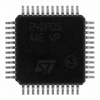
STP24DP05BTR STMicroelectronics, STP24DP05BTR Datasheet

STP24DP05BTR
Specifications of STP24DP05BTR
Available stocks
Related parts for STP24DP05BTR
STP24DP05BTR Summary of contents
Page 1
... GND, short open line. O Table 1. Device summary Order code STP24DP05BTR 1. Thermal pad size: 3 3.5 mm November 2009 The data detection results are loaded in the shift registers and shifted out via the serial line output. The detection functionality is activated with a dedicated pin or as alternative, through a logic sequence that allows the user to enter or exit from detection mode ...
Page 2
Contents Contents 1 Summary description . . . . . . . . . . . . . . . . . . . . . . . . . . . . . . . . . . . ...
Page 3
STP24DP05 1 Summary description Table 2. Current accuracy Output voltage ≥ 1.0 V ≥ 0.2 V 1.1 Pin connection and description Figure 1. Pin connection Note: The exposed pad should be electrically connected to a metal land electrically isolated or ...
Page 4
Summary description Table 3. Pin description Pin N° 12, 25, 30 13, 16, 19, 22, 39, 42, 45 15, 18, 21, 24 37, 40, 43 ...
Page 5
STP24DP05 2 Electrical ratings 2.1 Absolute maximum ratings Stressing the device above the rating listed in the “absolute maximum ratings” table may cause permanent damage to the device. These are stress ratings only and operation of the device at these ...
Page 6
Electrical ratings 2.3 Recommended operating conditions Table 6. Recommended operating conditions Symbol Parameter V Supply voltage DD V Output voltage O I Output current O I Output current OH I Output current OL V Input voltage IH V Input voltage ...
Page 7
STP24DP05 3 Electrical characteristics °C, unless otherwise specified. Table 7. Electrical characteristics (V Symbol Parameter V Input voltage high level IH V Input voltage low level IL I Output leakage current OH Output voltage V OL (Serial-OUT) ...
Page 8
Electrical characteristics Table 7. Electrical characteristics (V Symbol Parameter Thermal Thermal protection V Output voltage TF I Output current TF V Output voltage EF I Output current EF Table 8. Switching characteristics (V Symbol Parameter Propagation delay time, t PLH1 ...
Page 9
STP24DP05 4 Block diagram Figure 2. Block diagram Doc ID 14714 Rev 4 Block diagram 9/26 ...
Page 10
Equivalent circuit and outputs 5 Equivalent circuit and outputs Figure 3. OExx terminal Figure 4. LE\DM terminal Figure 5. CLK, SDI terminal 10/26 Doc ID 14714 Rev 4 STP24DP05 ...
Page 11
STP24DP05 Figure 6. SDO terminal Figure 7. TF and EF Equivalent circuit and outputs Doc ID 14714 Rev 4 11/26 ...
Page 12
Timing diagrams 6 Timing diagrams Figure 8. Timing diagram Note: 1 Latch and output enable are level sensitive and are not synchronized with rising-or-falling edge of CLK signal. 2 When LE\DM terminal is low level, the latch circuit hold previous ...
Page 13
STP24DP05 Figure 9. Clock, serial-in, serial-out Doc ID 14714 Rev 4 Timing diagrams 13/26 ...
Page 14
Timing diagrams Figure 10. Clock, serial-in, latch, enable, outputs Figure 11. Outputs 14/26 Doc ID 14714 Rev 4 STP24DP05 ...
Page 15
STP24DP05 7 Feature description 7.1 DG: gradual outputs delay This feature prevents large inrush current and reduces the bypass capacitors. The fixed delay time can be activated with DG = LOW and the typical output delay for ...
Page 16
Feature description Figure 12. Detection circuit 7.3 Phase one: “entering in detection mode” From the “normal mode” condition the device can switch to the “error detection mode” PIN set to LOW or a logic sequence on the ...
Page 17
STP24DP05 Figure 14. SPI sequence to enter in detection mode - time diagram OE-R\DM LE\DM After these five CLK cycles the device goes into the “error detection mode” and at the 6 rise front of CLK the SDI data are ...
Page 18
Feature description 7.5 Phase three: “resuming to normal mode” In order to re-enter in normal mode either the LE\DM pin or the sequence showed in the following table and diagram can be used: Table 13. SPI sequence to resume in ...
Page 19
STP24DP05 7.7 EFLAG/TFLAG - output detection and overtemperature monitoring The open-drain output EFLAG and TFLAG are used to report the STP24DP05 error flags. During normal operating conditions, the voltage on EFLAG/TFLAG is pulled-up through an external resistor. When an error ...
Page 20
Typical application schematic 8 Typical application schematic Figure 17. Typical application schematic 20/26 Doc ID 14714 Rev 4 STP24DP05 ...
Page 21
STP24DP05 9 Typical characteristics Figure 18. Typical external resistor values vs output current capabilities Table 15. Typical external resistor values vs output current capabilities Iset Rext (Ω) Figure 19. Typical dropout voltage vs output current Table 16. Typical dropout voltage ...
Page 22
Package mechanical data 10 Package mechanical data In order to meet environmental requirements, ST offers these devices in different grades of ® ECOPACK packages, depending on their level of environmental compliance. ECOPACK® specifications, grade definitions and product status are available ...
Page 23
STP24DP05 Figure 20. TQFP48-EP mechanical data Doc ID 14714 Rev 4 Package mechanical data 23/26 ...
Page 24
Package mechanical data Figure 21. Tape and reel TQFP48-EP DIM 24/26 Tape & Reel TQFP48 MECHANICAL DATA mm. MIN. TYP MAX. 330 12.8 13.2 20.2 60 22.4 9.5 9.7 9.5 ...
Page 25
STP24DP05 11 Revision history Table 18. Document revision history Date 19-Apr-2008 12-Jan-2009 04-Mar-2009 13-Nov-2009 Revision 1 First release 2 Updated package to TQFP48-EP 3 Updated Table 3 on page 4 4 Updated Table 3 on page 4 Doc ID 14714 ...
Page 26
... Information in this document is provided solely in connection with ST products. STMicroelectronics NV and its subsidiaries (“ST”) reserve the right to make changes, corrections, modifications or improvements, to this document, and the products and services described herein at any time, without notice. All ST products are sold pursuant to ST’s terms and conditions of sale. ...


