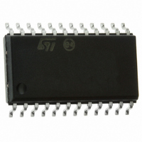
STP16CPPS05MTR STMicroelectronics, STP16CPPS05MTR Datasheet
STP16CPPS05MTR
Specifications of STP16CPPS05MTR
Available stocks


Related parts for STP16CPPS05MTR


STP16CPPS05MTR Summary of contents
Page 1
... D-type storage register. In the output stage, sixteen regulated current sources are designed to provide constant current to drive the LEDs. Table 1. Device summary Order codes STP16CPPS05MTR STP16CPPS05TTR STP16CPPS05XTTR STP16CPPS05PTR October 2009 This is preliminary information on a new product now in development or undergoing evaluation. Details are subject to change without notice. ...
Page 2
Contents Contents 1 Summary description . . . . . . . . . . . . . . . . . . . . . . . . . . . . . . . . . . . ...
Page 3
STP16CPPS05 1 Summary description Table 2. Typical current accuracy Output voltage ≥ 1.3 V 1.1 Pin connection and description Figure 1. Pin connection Note: The exposed pad should be electrically connected to a metal land electrically isolated or connected to ...
Page 4
Summary description Table 3. Pin description Pin n° 5-20 OUT 0- 4/29 Symbol GND Ground terminal SDI Serial data input terminal CLK Clock input terminal LE Latch input terminal - detect mode ...
Page 5
STP16CPPS05 2 Electrical ratings 2.1 Absolute maximum ratings Stressing the device above the ratings listed in the “absolute maximum ratings” table may cause permanent damage to the device. These are stress ratings only and operation of the device at these ...
Page 6
Electrical ratings 2.3 Recommended operating conditions Table 6. Recommended operating conditions Symbol Parameter V Supply voltage DD V Output voltage O I Output current O I Output current OH I Output current OL V Input voltage IH V Input voltage ...
Page 7
STP16CPPS05 3 Electrical characteristics Table 7. Electrical characteristics Symbol V Input voltage high level IH V Input voltage low level IL I Output leakage current OH Output voltage V OL (serial-OUT) ...
Page 8
Electrical characteristics Table 8. Switching characteristics Symbol Parameter Propagation delay time, t PLH1 CLK-OUTn Propagation delay time, t LE-OUTn, PLH2 Propagation delay ...
Page 9
STP16CPPS05 4 Equivalent circuit and outputs Figure 2. OE terminal Figure 3. LE terminal Figure 4. CLK, SDI terminal Equivalent circuit and outputs Doc ID 16536 Rev 1 9/29 ...
Page 10
Equivalent circuit and outputs Figure 5. SDO terminal Figure 6. Block diagram 10/29 Doc ID 16536 Rev 1 STP16CPPS05 ...
Page 11
STP16CPPS05 5 Timing diagrams Table 9. Truth table CLOCK Note: OUTn = ON when OUTn = OFF when Figure 7. Timing diagram Note: 1 Latch and output enable ...
Page 12
Timing diagrams Table 10. Enable IO: shutdown truth table CLOCK power-up, the device starts in shutdown mode. 2. Undefined. Figure 8. Clock, serial-in, serial-out 12/29 SDI ........... SDI ............ SDI All ...
Page 13
STP16CPPS05 Figure 9. Clock, serial-in, latch, enable, outputs LE OE OUTn Figure 10. Outputs OUTn Doc ID 16536 Rev 1 Timing diagrams 13/29 ...
Page 14
Typical characteristics 6 Typical characteristics Figure 11. Output current vs. R-EXT resistor Table 11. Output current vs. R-EXT resistor 14/29 25000 20000 15000 10000 5000 Current (mA) R-EXT (Ω) 23700 11730 6930 4090 2025 1000 ...
Page 15
STP16CPPS05 Conditions: Temperature = 25 °C, V Figure 12. I SET 1200 1000 800 600 400 200 Table 12. I SET Iout (mA 3 mA; 5 mA; ...
Page 16
Typical characteristics °C, Vdd = 3 Figure 13. Output current vs. ± ΔI Figure 14. Idd ON/OFF 16/29 (%) ...
Page 17
STP16CPPS05 Figure 15. Power dissipation vs. package temperature Note: The exposed pad should be soldered to the PCB to obtain the thermal benefits. Figure 16. Turn ON output current characteristics Electrical conditions: Vdd = 3.3 V, Vin = Vdd, Vled ...
Page 18
Typical characteristics 6.1 Auto power-saving The auto power-saving feature minimizes the quiescent current if no active data is detected on the latches and auto powers-up the device as the first active data is latched. Figure 18. Auto power-saving feature Electrical ...
Page 19
STP16CPPS05 Figure 19. First output ON after switching from auto power saving to normal operating condition Electrical conditions: temp °C, Vdd = 3.3 V, Vin = Vdd, Vled = 3.0 V, Iset = 20 mA Ch1 (Yellow) = ...
Page 20
Package mechanical data 7 Package mechanical data In order to meet environmental requirements, ST offers these devices in different grades of ® ECOPACK packages, depending on their level of environmental compliance. ECOPACK® specifications, grade definitions and product status are available ...
Page 21
STP16CPPS05 Figure 20. QSOP-24 package dimensions Doc ID 16536 Rev 1 Package mechanical data 21/29 ...
Page 22
Package mechanical data Table 14. QSOP-24 tape and reel Dim eint e1 Figure 21. QSOP-24 tape and reel dimensions 0.3+/-0.05 0.3+/-0.05 22/29 mm. Min Typ Max 12.8 13 13.5 330 100 16.4 1.5 2 2.5 2.0+/-0.1 2.0+/-0.1 ...
Page 23
STP16CPPS05 Table 15. TSSOP24 mechanical data Dim Figure 22. TSSOP24 package dimensions mm. Min Typ Max 1.1 0.05 0.15 0.9 0.19 0.30 0.09 0.20 7.7 7.9 4.3 4.5 0.65 ...
Page 24
Package mechanical data Table 16. TSSOP24 exposed pad mechanical data Dim Figure 23. TSSOP24 exposed pad dimensions 24/29 mm Min Typ Max 1.2 0.15 0.8 1 1.05 ...
Page 25
STP16CPPS05 Table 17. Tape and reel TSSOP24 and TSSOP24 exposed pad Dim Figure 24. TSSOP24 and TSSOP24 exposed pad tape and reel dimensions mm. Min Typ Max 330 12.8 13.2 ...
Page 26
Package mechanical data Table 18. SO-24 mechanical data Dim Figure 25. SO-24 package dimensions 26/29 mm. Min Typ Max 2.65 0.1 0.2 2.45 0.35 0.49 0.23 ...
Page 27
STP16CPPS05 Table 19. Tape and reel SO-24 Dim Figure 26. SO-24 tape and reel dimensions mm. Min Typ Max 330 12.8 13.2 20.2 60 30.4 10.8 11.0 15.7 15.9 2.9 ...
Page 28
Revision history 8 Revision history Table 20. Document revision history Date 23-Oct-2009 28/29 Revision 1 Initial release. Doc ID 16536 Rev 1 STP16CPPS05 Changes ...
Page 29
... STP16CPPS05 Information in this document is provided solely in connection with ST products. STMicroelectronics NV and its subsidiaries (“ST”) reserve the right to make changes, corrections, modifications or improvements, to this document, and the products and services described herein at any time, without notice. All ST products are sold pursuant to ST’s terms and conditions of sale. ...