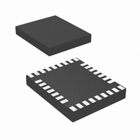
LP3950SL/NOPB National Semiconductor, LP3950SL/NOPB Datasheet - Page 16

LP3950SL/NOPB
Manufacturer Part Number
LP3950SL/NOPB
Description
IC LED DRVR WHITE BCKLGT 32-TSCP
Manufacturer
National Semiconductor
Series
PowerWise®r
Type
Backlight, White LED (I²C Interface)r
Datasheet
1.LP3950SLNOPB.pdf
(31 pages)
Specifications of LP3950SL/NOPB
Topology
PWM, Step-Up (Boost)
Number Of Outputs
6
Internal Driver
Yes
Type - Primary
Flash/Torch, LED Blinker, Light Management Unit (LMU)
Type - Secondary
RGB, White LED
Frequency
2MHz
Voltage - Supply
2.7 V ~ 2.9 V
Voltage - Output
5V
Mounting Type
Surface Mount
Package / Case
32-Laminate TCSP
Operating Temperature
-40°C ~ 85°C
Internal Switch(s)
Yes
Efficiency
90%
Led Driver Application
Mobile Phone Display Lighting, General LED Lighting
No. Of Outputs
6
Output Current
300mA
Output Voltage
5.3V
Input Voltage
3V To 7.2V
Rohs Compliant
Yes
Lead Free Status / RoHS Status
Lead free / RoHS Compliant
Current - Output / Channel
-
Other names
LP3950SL/CSP1
LP3950SLTR
LP3950SLTR
www.national.com
Boost Converter Typical Performance Characteristics
otherwise stated. (Continued)
RGB LED Pattern Generator
The LP3950 RGB outputs can be controlled either with audio
synchronization or with RGB pattern generator.
The pattern generator of LP3950 drives three independently
controlled LED outputs (for example, R1, G1 and B1). The
functionality is similar compared to RGB functionality of
LP3936 and LP3933.
The output of RGB pattern generator can be selected to
drive RGB1 (R1-G1-B1), RGB2 (R2-G2-B2) or RGB1 and
RGB2 (R1&R2 – G1&G2 – B1&B2) outputs.
Programmable Pattern Mode
User has control over the following parameters separately
for each LED:
The main blinking cycle is controlled with three-bit CYCLE
control (0.25 / 0.5 / 1.0 / 2.0 / 4.0s).
RGB_START is the master control for the whole RGB func-
tion. The internal PWM and blinking control can be disabled
by setting the RGB_PWM control LOW. In this case the
individual enable controls can be used to switch outputs on
and off. PWM_EN input can be used for external hardware
PWM control.
• ON and OFF (start and stop time in blinking cycle)
• DUTY
• SLOPE
• ENABLE
FIGURE 12. RGB PWM Operating Principle
(PWM brightness control)
(dimming slope)
(output enable control)
Boost Line Regulation
20129319
20129324
16
In the normal PWM mode the R, G and B switches are
controlled in 3 phases (one phase per driver). During each
phase the peak current set by an external ballast resistor is
driven through the LED for the time defined by DUTY setting
(0 µs to 50 µs). As a time averaged current this means
0% to 33% of the peak current. The PWM period is 150 µs
and the pulse frequency is 6.67 kHz in normal mode.
In the FLASH mode all the outputs are controlled in one
phase and the PWM period is 50 µs. The time averaged
FLASH mode current is three times the normal mode current
at the same DUTY value.
FIGURE 13. Normal Mode PWM Waveforms at Different
Boost Load Transient Response, 50 mA to 100 mA
Duty Settings
V
IN
= 3.6V, V
OUT
20129323
= 5.0V if not
20129325


