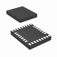
LP3950SL/NOPB National Semiconductor, LP3950SL/NOPB Datasheet - Page 8

LP3950SL/NOPB
Manufacturer Part Number
LP3950SL/NOPB
Description
IC LED DRVR WHITE BCKLGT 32-TSCP
Manufacturer
National Semiconductor
Series
PowerWise®r
Type
Backlight, White LED (I²C Interface)r
Datasheet
1.LP3950SLNOPB.pdf
(31 pages)
Specifications of LP3950SL/NOPB
Topology
PWM, Step-Up (Boost)
Number Of Outputs
6
Internal Driver
Yes
Type - Primary
Flash/Torch, LED Blinker, Light Management Unit (LMU)
Type - Secondary
RGB, White LED
Frequency
2MHz
Voltage - Supply
2.7 V ~ 2.9 V
Voltage - Output
5V
Mounting Type
Surface Mount
Package / Case
32-Laminate TCSP
Operating Temperature
-40°C ~ 85°C
Internal Switch(s)
Yes
Efficiency
90%
Led Driver Application
Mobile Phone Display Lighting, General LED Lighting
No. Of Outputs
6
Output Current
300mA
Output Voltage
5.3V
Input Voltage
3V To 7.2V
Rohs Compliant
Yes
Lead Free Status / RoHS Status
Lead free / RoHS Compliant
Current - Output / Channel
-
Other names
LP3950SL/CSP1
LP3950SLTR
LP3950SLTR
www.national.com
LOGIC INPUTS DME, AMODE (Internal pull down 1 MΩ)
I
LOGIC INPUTS SCL, PWM_LED, IF_SEL
V
V
I
f
LOGIC I/O SDA
V
LOGIC INPUTS DME, AMODE (Internal pull down 1 MΩ)
V
V
I
V
V
I
t
I
I
SCL
I
I
NRST
Logic Interface Characteristics
IL
IH
OL
IL
IH
IL
IH
IF_SEL
(1.80V ≤ V
ambient temperature range (−40˚C ≤ T
Logic Interface Characteristics, Low I/O Voltage
(1.65V ≤ V
Logic Input NRST Characteristics
(1.65V ≤ V
Control Interface
The LP3950 supports three different interface modes:
1) SPI interface (4 wire, serial)
2) I
3) Direct enable (2 wire, enable lines)
SPI Interface
The transmission consists of 16-bit write and read cycles.
One cycle consists of seven address bits, one read/write
(R/W) bit and eight data bits. R/W bit high state defines a
write cycle and low defines a read cycle. SO output is
normally in high-impedance state and it is active only during
Symbol
Symbol
Symbol
HIGH
LOW
2
C compatible interface (2 wire, serial)
DDIO
DDIO
DDIO
SPI
I
2
Logic Input Current
Input Low Level
Input High Level
Logic Input Current
Clock Frequency
Output Low Level
Input Low Level
Input High Level
Logic Input Current
Input Low Level
Input High Level
Logic Input Current
Reset Pulse Width
C Compatible
Interface
≤ V
≤ V
<
1.80V) . I
Parameter
Parameter
Parameter
DD1,2
DD1,2
V). Limits in standard typeface are for T
V).
2
C compatible interface only.
SCK
SI
SO
SS
SCL
SDA
SI
SO
Pin Configuration
A
I
I
Note: Guaranteed by
design
2
SDA
C Mode
≤ +85˚C).
= 3.0 mA
Conditions
Conditions
Conditions
(clock)
(data in)
(data out)
(chip select)
(clock)
(data in/out)
(I
(NC)
2
address)
(Continued)
8
J
Use pull up resistor for SCL.
Use pull up resistor for SDA.
SI HIGH → address is 51’h;
SI LOW → address is 50’h;
Unused pin SO can be left unconnected.
= +25˚C. Limits in boldface type apply over the operating
User can define the serial interface by the IF_SEL pin. The
following table shows the pin configuration for both interface
modes. Note that the pin configurations will be based on the
status of the IF_SEL pin.
when data is sent out during a read cycle. A pull-up or
pull-down resistor may be needed for SO line if a floating
logic signal can cause unintended current consumption in
the circuitry.
The address and data are transmitted Most Significant Byte
(MSB) first. The Slave Select signal (SS) must be low during
the cycle transmission. SS resets the interface when high
V
V
DDIO
DDIO
−1.0
−1.0
−1.0
−1.0
Min
Min
Min
1.3
10
− 0.35
− 0.35
Comment
Typ
Typ
Typ
0.3
Max
Max
0.35
0.35
Max
200
6.0
1.0
0.5
6.0
0.5
1.0
Units
Units
Units
kHz
µA
µA
µA
µA
µs
V
V
V
V
V
V
V


