LM3554TME/NOPB National Semiconductor, LM3554TME/NOPB Datasheet - Page 18
LM3554TME/NOPB
Manufacturer Part Number
LM3554TME/NOPB
Description
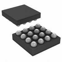
IC LED DVR PHOTO FLASH 16-USMD
Manufacturer
National Semiconductor
Type
Photo Flash LED (I²C Interface)r
Datasheet
1.LM3554TMENOPB.pdf
(40 pages)
Specifications of LM3554TME/NOPB
Constant Current
Yes
Topology
High Side, Step-Up (Boost)
Number Of Outputs
2
Internal Driver
Yes
Type - Primary
Flash/Torch
Type - Secondary
White LED
Frequency
2MHz
Voltage - Supply
2.7 V ~ 5.5 V
Voltage - Output
5V
Mounting Type
Surface Mount
Package / Case
16-MicroSMD
Operating Temperature
-30°C ~ 85°C
Current - Output / Channel
600mA
Internal Switch(s)
Yes
Efficiency
90%
Led Driver Application
LED Backlighting, Portable Electronics
No. Of Outputs
2
Output Current
1.2A
Input Voltage
2.7V To 5.5V
Dimming Control Type
I2C
Rohs Compliant
Yes
Lead Free Status / RoHS Status
Lead free / RoHS Compliant
Other names
LM3554TMETR


www.national.com
Maximum Output Power (Led Boost Mode)
In LED mode with V
will switch and make V
total power dissipated in the LM3554 is approximated as:
Maximum Output Power (Led Pass Mode)
In LED mode with V
LM3554 operates in Pass Mode. In this case. the NFET is off,
Once the total power dissipated in the LM3554 is calculated
the ambient temperature and the thermal resistance of the 16-
bump micro SMD (TMD16) are used to calculate the total die
temperature (or junction temperature T
As an example, assume the LM3554 is operating at V
and configured for Voltage Output mode with V
I
mode with 150mA each at V
dicator LED has 10mA at V
2 above, the approximate total power dissipated in the device
is:
The die temperature approximation will be:
In this case the device can operate at these conditions. If then
the ambient temperature is increased to +85°C, the die tem-
perature would be +140.8°C; thus, the die temperature would
OUT
= 0.7A. The LED currents are then programmed in Torch
OUT
IN
OUT
– I
> V
= V
LOAD
IND
IN
LED
LED
= 3.6V. Using Equations 1 and
the LM3554’s boost converter
× R
= 3.6V. Additionally, the in-
+ 0.3V. In this situation the
PFET
J
).
> V
LED
OUT
+ 0.3V, the
= 5V and
IN
= 3.6V
Equation 1
Equation 2
18
and the PFET is fully on. The difference between
V
sources. In this situation the total power dissipated in the
LM3554 is approximated as:
be above the absolute maximum ratings, and the load current
would need to be scaled back. This example demonstrates
the steps required to estimate the amount of current derating
based upon operating mode, circuit parameters, and the
device's junction-toambient thermal resistance. In this exam-
ple a thermal resistance of 60°C/W was used (JESD51-7
standard). Since thermal resistance from junction-to-ambient
is largely PCB layout dependent, the actual number used will
likely be different and must be taken into account when per-
forming these calculations.
FLASH MODE
In Flash mode the LED current sources (LED1 and LED2)
each provide 16 different current levels from typically 34mA
to approximately 600mA. The Flash currents are set by writing
to bits [6:3] of the Flash Brightness Resister. Flash mode is
activated by either writing a (1, 1) to bits [1:0] of the Torch
Brightness Register, writing a (1,1) to bit [1:0] of the Flash
Brightness Register, or by pulling the STROBE pin high. Once
the Flash sequence is activated, both current sinks (LED1 and
LED2) will ramp up to the programmed Flash current by step-
ping through all Flash levels (16µs/step) until the programmed
current is reached.
IN
- I
LOAD
×R
PMOS
and V
LED
will be dropped across the current
30042012
30042011
Related parts for LM3554TME/NOPB
Image
Part Number
Description
Manufacturer
Datasheet
Request
R

Part Number:
Description:
LM3554 PRODUCT BRIEF Synchronous Boost Converter with 1.2A Dual High Side LED Drivers and I<sup>2</sup>C Compatible Interface; Package: MICRO SMD; No of Pins: 16; Qty per Container: 250/Reel
Manufacturer:
National Semiconductor
Part Number:
Description:
National Semiconductor [8-Bit D/A Converter]
Manufacturer:
National Semiconductor
Datasheet:
Part Number:
Description:
National Semiconductor [Media Coprocessor]
Manufacturer:
National Semiconductor
Datasheet:
Part Number:
Description:
Digitally Controlled Tone and Volume Circuit with Stereo Audio Power Amplifier, Microphone Preamp Stage and National 3D Sound
Manufacturer:
National Semiconductor
Datasheet:
Part Number:
Description:
Digitally Controlled Tone and Volume Circuit with Stereo Audio Power Amplifier, Microphone Preamp Stage and National 3D Sound
Manufacturer:
National Semiconductor
Datasheet:
Part Number:
Description:
AC97 Rev 2 Codec with Sample Rate Conversion and National 3D Sound
Manufacturer:
National Semiconductor
Part Number:
Description:
Manufacturer:
National Semiconductor
Datasheet:
Part Number:
Description:
Manufacturer:
National Semiconductor
Datasheet:
Part Number:
Description:
General Purpose, Low Voltage, Low Power, Rail-to-Rail Output Operational Amplifiers
Manufacturer:
National Semiconductor
Datasheet:
Part Number:
Description:
8-bit 20 MSPS flash A/D converter.
Manufacturer:
National Semiconductor
Datasheet:
Part Number:
Description:
Low Noise Quad Operational Amplifier
Manufacturer:
National Semiconductor
Datasheet:
Part Number:
Description:
Quad Differential Line Receivers
Manufacturer:
National Semiconductor
Datasheet:
Part Number:
Description:
Quad High Speed Trapezoidal? Bus Transceiver
Manufacturer:
National Semiconductor
Datasheet:
Part Number:
Description:
Dual Line Receiver
Manufacturer:
National Semiconductor
Datasheet: