LM3554TME/NOPB National Semiconductor, LM3554TME/NOPB Datasheet - Page 5
LM3554TME/NOPB
Manufacturer Part Number
LM3554TME/NOPB
Description
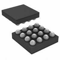
IC LED DVR PHOTO FLASH 16-USMD
Manufacturer
National Semiconductor
Type
Photo Flash LED (I²C Interface)r
Datasheet
1.LM3554TMENOPB.pdf
(40 pages)
Specifications of LM3554TME/NOPB
Constant Current
Yes
Topology
High Side, Step-Up (Boost)
Number Of Outputs
2
Internal Driver
Yes
Type - Primary
Flash/Torch
Type - Secondary
White LED
Frequency
2MHz
Voltage - Supply
2.7 V ~ 5.5 V
Voltage - Output
5V
Mounting Type
Surface Mount
Package / Case
16-MicroSMD
Operating Temperature
-30°C ~ 85°C
Current - Output / Channel
600mA
Internal Switch(s)
Yes
Efficiency
90%
Led Driver Application
LED Backlighting, Portable Electronics
No. Of Outputs
2
Output Current
1.2A
Input Voltage
2.7V To 5.5V
Dimming Control Type
I2C
Rohs Compliant
Yes
Lead Free Status / RoHS Status
Lead free / RoHS Compliant
Other names
LM3554TMETR


Note 1: Absolute Maximum Ratings indicate limits beyond which damage to the device may occur. Operating Ratings are conditions under which operation of
the device is guaranteed. Operating Ratings do not imply guaranteed performance limits. For guaranteed performance limits and associated test conditions, see
the Electrical Characteristics table.
Note 2: All voltages are with respect to the potential at the GND pin.
Note 3: Internal thermal shutdown circuitry protects the device from permanent damage. Thermal shutdown engages at T
T
Note 4: For detailed soldering specifications and information, please refer to National Semiconductor Application Note 1112: Micro SMD Wafer Level chip Scale
Package (AN-1112)
Note 5: In applications where high power dissipation and/or poor package thermal resistance is present, the maximum ambient temperature may have to be
derated. Maximum ambient temperature (T
dissipation of the device in the application (P
following equation: T
Note 6: Junction-to-ambient thermal resistance (θ
JEDEC standard JESD51-7. The test board is a 4-layer FR-4 board measuring 102mm x 76mm x 1.6mm with a 2x1 array of thermal via's. The ground plane on
the board is 50mm x 50mm. Thickness of copper layers are 36µm/18µm/18µm/36µm (1.5oz/1oz/1oz/1.5oz). Ambient temperature in simulation is 22°C, still air.
Power dissipation is 1W.
Note 7: Min and Max limits are guaranteed by design, test, or statistical analysis. Typical (Typ) numbers are not guaranteed, but do represent the most likely
norm. Unless otherwise specified, conditions for typical specifications are: V
Note 8: The typical curve for Over-Voltage Protection (OVP) is measured in closed loop using the typical application circuit . The OVP value is found by forcing
an open circuit in the LED1 and LED2 path and recording the peak value of V
by ramping the voltage at OUT until the OVP comparator trips. The closed loop data can appear higher due to the stored energy in the inductor being dumped
into the output capacitor after the OVP comparator trips. At worst case is an open circuit condition where the output voltage can continue to rise after the OVP
comparator trips by approximately I
Note 9: The typical curve for Current Limit is measured in closed loop using the typical application circuit by increasing I
increasing. The value given in the Electrical Table is measured open loop and is found by forcing current into SW until the current limit comparator threshold is
reached. Closed loop data appears higher due to the delay between the comparator trip point and the NFET turning off. This delay allows the closed loop inductor
current to ramp higher after the trip point by approximately 20ns × V
Note 10: Current Matching = Absolute Value((I
Note 11: Current Accuracy = Absolute Value(I
J
=135°C (typ.).
A-MAX
= T
J-MAX-OP
IN
×sqrt(L/C
– (θ
JA
A-MAX
× P
D-MAX
OUT
TARGET
LED1
D-MAX
) is dependent on the maximum operating junction temperature (T
).
), and the junction-to-ambient thermal resistance of the part/package in the application (θ
JA
- I
) is taken from a thermal modeling result, performed under the conditions and guidelines set forth in the
).
- (I
LED2
LED1
)/(I
LED1
+ I
LED2
+ I
FIGURE 1. I
)) × 100
IN
LED2
/L
)) × 100
IN
OUT
= 3.6V and T
5
2
. The value given in the Electrical Table is found in an open loop configuration
C Timing
A
= +25°C.
J-MAX-OP
OUT
J
=150°C (typ.) and disengages at
= +125°C), the maximum power
until the peak inductor current stops
30042004
JA
), as given by the
www.national.com
Related parts for LM3554TME/NOPB
Image
Part Number
Description
Manufacturer
Datasheet
Request
R

Part Number:
Description:
LM3554 PRODUCT BRIEF Synchronous Boost Converter with 1.2A Dual High Side LED Drivers and I<sup>2</sup>C Compatible Interface; Package: MICRO SMD; No of Pins: 16; Qty per Container: 250/Reel
Manufacturer:
National Semiconductor
Part Number:
Description:
National Semiconductor [8-Bit D/A Converter]
Manufacturer:
National Semiconductor
Datasheet:
Part Number:
Description:
National Semiconductor [Media Coprocessor]
Manufacturer:
National Semiconductor
Datasheet:
Part Number:
Description:
Digitally Controlled Tone and Volume Circuit with Stereo Audio Power Amplifier, Microphone Preamp Stage and National 3D Sound
Manufacturer:
National Semiconductor
Datasheet:
Part Number:
Description:
Digitally Controlled Tone and Volume Circuit with Stereo Audio Power Amplifier, Microphone Preamp Stage and National 3D Sound
Manufacturer:
National Semiconductor
Datasheet:
Part Number:
Description:
AC97 Rev 2 Codec with Sample Rate Conversion and National 3D Sound
Manufacturer:
National Semiconductor
Part Number:
Description:
Manufacturer:
National Semiconductor
Datasheet:
Part Number:
Description:
Manufacturer:
National Semiconductor
Datasheet:
Part Number:
Description:
General Purpose, Low Voltage, Low Power, Rail-to-Rail Output Operational Amplifiers
Manufacturer:
National Semiconductor
Datasheet:
Part Number:
Description:
8-bit 20 MSPS flash A/D converter.
Manufacturer:
National Semiconductor
Datasheet:
Part Number:
Description:
Low Noise Quad Operational Amplifier
Manufacturer:
National Semiconductor
Datasheet:
Part Number:
Description:
Quad Differential Line Receivers
Manufacturer:
National Semiconductor
Datasheet:
Part Number:
Description:
Quad High Speed Trapezoidal? Bus Transceiver
Manufacturer:
National Semiconductor
Datasheet:
Part Number:
Description:
Dual Line Receiver
Manufacturer:
National Semiconductor
Datasheet: