LM3554TME/NOPB National Semiconductor, LM3554TME/NOPB Datasheet - Page 26
LM3554TME/NOPB
Manufacturer Part Number
LM3554TME/NOPB
Description
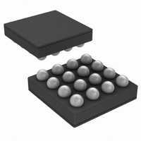
IC LED DVR PHOTO FLASH 16-USMD
Manufacturer
National Semiconductor
Type
Photo Flash LED (I²C Interface)r
Datasheet
1.LM3554TMENOPB.pdf
(40 pages)
Specifications of LM3554TME/NOPB
Constant Current
Yes
Topology
High Side, Step-Up (Boost)
Number Of Outputs
2
Internal Driver
Yes
Type - Primary
Flash/Torch
Type - Secondary
White LED
Frequency
2MHz
Voltage - Supply
2.7 V ~ 5.5 V
Voltage - Output
5V
Mounting Type
Surface Mount
Package / Case
16-MicroSMD
Operating Temperature
-30°C ~ 85°C
Current - Output / Channel
600mA
Internal Switch(s)
Yes
Efficiency
90%
Led Driver Application
LED Backlighting, Portable Electronics
No. Of Outputs
2
Output Current
1.2A
Input Voltage
2.7V To 5.5V
Dimming Control Type
I2C
Rohs Compliant
Yes
Lead Free Status / RoHS Status
Lead free / RoHS Compliant
Other names
LM3554TMETR


www.national.com
I
START AND STOP CONDITIONS
The LM3554 is controlled via an I
START and STOP conditions classify the beginning and end
of the I
The I
free after a STOP condition. During data transmission the
I
START and a repeated START condition are equivalent func-
tion-wise. The data on SDA must be stable during the HIGH
I
The device address for the LM3554 is 1010011 (53). After the
START condition, the I
lowed by an eighth bit, read or write (R/W). R/W = 0 indicates
2
2
2
C master can generate repeated START conditions. A
C-COMPATIBLE CHIP ADDRESS
C-Compatible Interface
2
C bus is considered busy after a START condition and
2
C session. A START condition is defined as SDA
2
C master sends the 7-bit address fol-
2
C-compatible interface.
FIGURE 13. Start and Stop Sequences
FIGURE 14. I
FIGURE 15. Device Address
2
C-Compatible Timing
26
transitioning from HIGH to LOW while SCL is HIGH. A STOP
condition is defined as SDA transitioning from LOW to HIGH
while SCL is HIGH. The I
START and STOP conditions.
period of the clock signal (SCL). In other words, the state of
SDA can only be changed when SCL is LOW.
Figure 14
Compatible Bus. See the Electrical Characteristics Table for
timing values.
a WRITE and R/W = 1 indicates a READ. The second byte
following the device address selects the register address to
which the data will be written. The third byte contains the data
for the selected register.
show the SDA and SCL signal timing for the I
2
C master always generates the
30042019
30042018
30042020
Figure 1
and
2
C-
Related parts for LM3554TME/NOPB
Image
Part Number
Description
Manufacturer
Datasheet
Request
R

Part Number:
Description:
LM3554 PRODUCT BRIEF Synchronous Boost Converter with 1.2A Dual High Side LED Drivers and I<sup>2</sup>C Compatible Interface; Package: MICRO SMD; No of Pins: 16; Qty per Container: 250/Reel
Manufacturer:
National Semiconductor
Part Number:
Description:
National Semiconductor [8-Bit D/A Converter]
Manufacturer:
National Semiconductor
Datasheet:
Part Number:
Description:
National Semiconductor [Media Coprocessor]
Manufacturer:
National Semiconductor
Datasheet:
Part Number:
Description:
Digitally Controlled Tone and Volume Circuit with Stereo Audio Power Amplifier, Microphone Preamp Stage and National 3D Sound
Manufacturer:
National Semiconductor
Datasheet:
Part Number:
Description:
Digitally Controlled Tone and Volume Circuit with Stereo Audio Power Amplifier, Microphone Preamp Stage and National 3D Sound
Manufacturer:
National Semiconductor
Datasheet:
Part Number:
Description:
AC97 Rev 2 Codec with Sample Rate Conversion and National 3D Sound
Manufacturer:
National Semiconductor
Part Number:
Description:
Manufacturer:
National Semiconductor
Datasheet:
Part Number:
Description:
Manufacturer:
National Semiconductor
Datasheet:
Part Number:
Description:
General Purpose, Low Voltage, Low Power, Rail-to-Rail Output Operational Amplifiers
Manufacturer:
National Semiconductor
Datasheet:
Part Number:
Description:
8-bit 20 MSPS flash A/D converter.
Manufacturer:
National Semiconductor
Datasheet:
Part Number:
Description:
Low Noise Quad Operational Amplifier
Manufacturer:
National Semiconductor
Datasheet:
Part Number:
Description:
Quad Differential Line Receivers
Manufacturer:
National Semiconductor
Datasheet:
Part Number:
Description:
Quad High Speed Trapezoidal? Bus Transceiver
Manufacturer:
National Semiconductor
Datasheet:
Part Number:
Description:
Dual Line Receiver
Manufacturer:
National Semiconductor
Datasheet: