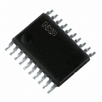
PCA9634PW,112 NXP Semiconductors, PCA9634PW,112 Datasheet - Page 2

PCA9634PW,112
Manufacturer Part Number
PCA9634PW,112
Description
IC LED DRIVER RGBA 20-TSSOP
Manufacturer
NXP Semiconductors
Type
RGBA LED Driverr
Datasheet
1.PCA9634D118.pdf
(38 pages)
Specifications of PCA9634PW,112
Package / Case
20-TSSOP
Topology
Open Drain, PWM
Number Of Outputs
8
Internal Driver
Yes
Type - Primary
Backlight, LED Blinker
Type - Secondary
RGBA
Frequency
1MHz
Voltage - Supply
2.3 V ~ 5.5 V
Voltage - Output
5.5V
Mounting Type
Surface Mount
Operating Temperature
-40°C ~ 85°C
Current - Output / Channel
25mA
Internal Switch(s)
Yes
Low Level Output Current
25 mA
High Level Output Current
50 uA
Operating Supply Voltage
2.3 V to 5.5 V
Maximum Supply Current
10 mA
Maximum Power Dissipation
400 mW
Maximum Operating Temperature
+ 85 C
Mounting Style
SMD/SMT
Minimum Operating Temperature
- 40 C
Lead Free Status / RoHS Status
Lead free / RoHS Compliant
Efficiency
-
Lead Free Status / Rohs Status
Details
Other names
935282233112
PCA9634PW
PCA9634PW
PCA9634PW
PCA9634PW
NXP Semiconductors
2. Features
PCA9634_6
Product data sheet
I
I
I
I
I
I
I
I
I
I
I
I
I
I
I
I
I
I
I
I
I
I
I
I
8 LED drivers. Each output programmable at:
1 MHz Fast-mode Plus compatible I
on SDA output for driving high capacitive buses
256-step (8-bit) linear programmable brightness per LED output varying from fully off
(default) to maximum brightness using a 97 kHz PWM signal
256-step group brightness control allows general dimming (using a 190 Hz PWM
signal) from fully off to maximum brightness (default)
256-step group blinking with frequency programmable from 24 Hz to 10.73 s and duty
cycle from 0 % to 99.6 %
Eight totem-pole outputs (sink 25 mA and source 10 mA at 5 V) with software
programmable open-drain LED outputs selection (default at totem-pole). No input
function.
Output state change programmable on the Acknowledge or the STOP Command to
update outputs byte-by-byte or all at the same time (default to ‘Change on STOP’).
Active LOW Output Enable (OE) input pin. LED outputs programmable to 1, 0 or
‘high-impedance’ (default at power-up) when OE is HIGH, thus allowing hardware
blinking and dimming of the LEDs.
7 hardware address pins allow 126 devices to be connected to the same I
4 software programmable I
LED Sub Call addresses) allow groups of devices to be addressed at the same time in
any combination (for example, one register used for ‘All Call’ so that all the PCA9634s
on the I
three different addresses so that
same time in a group). Software enable and disable for I
Software Reset feature (SWRST Call) allows the device to be reset through the
I
25 MHz internal oscillator requires no external components
Internal power-on reset
Noise filter on SDA/SCL inputs
Edge rate control on outputs
No glitch on power-up
Supports hot insertion
Low standby current
Operating power supply voltage range of 2.3 V to 5.5 V
5.5 V tolerant inputs
ESD protection exceeds 2000 V HBM per JESD22-A114, 200 V MM per
JESD22-A115, and 1000 V CDM per JESD22-C101
Latch-up testing is done to JEDEC Standard JESD78 which exceeds 100 mA
Packages offered: SO20, TSSOP20, HVQFN20
2
N
N
N
N
40 C to +85 C operation
C-bus
Off
On
Programmable LED brightness
Programmable group dimming/blinking mixed with individual LED brightness
2
C-bus can be addressed at the same time and the second register used for
Rev. 06 — 12 September 2008
2
C-bus addresses (one LED Group Call address and three
1
3
2
of all devices on the bus can be addressed at the
C-bus interface with 30 mA high drive capability
8-bit Fm+ I
2
C-bus address.
PCA9634
2
© NXP B.V. 2008. All rights reserved.
C-bus LED driver
2
C-bus
2 of 38


