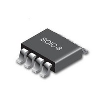
CY8CLEDAC02 Cypress Semiconductor Corp, CY8CLEDAC02 Datasheet - Page 12

CY8CLEDAC02
Manufacturer Part Number
CY8CLEDAC02
Description
IC CTLR AC-DC DIMMABLE LED 8SOIC
Manufacturer
Cypress Semiconductor Corp
Type
High Power, AC Input, Dimmabler
Datasheet
1.CY8CLEDAC02.pdf
(20 pages)
Specifications of CY8CLEDAC02
Package / Case
8-SOIC (3.9mm Width)
Voltage - Supply
8 V ~ 16 V
Frequency
200kHz
Operating Temperature
-40°C ~ 85°C
Number Of Outputs
1
Internal Switch(s)
No
Efficiency
85%
Topology
AC DC Offline Switcher
Operating Supply Voltage
- 0.3 V to 18 V
Maximum Supply Current
20 mA
Maximum Power Dissipation
526 mW
Maximum Operating Temperature
+ 85 C
Mounting Style
SMD/SMT
Minimum Operating Temperature
- 40 C
Operating Temperature (min)
-40C
Operating Temperature (max)
85C
Operating Temperature Classification
Industrial
Pin Count
8
Mounting
Surface Mount
Operating Supply Voltage (max)
18V
Lead Free Status / RoHS Status
Lead free / RoHS Compliant
Voltage - Output
-
Current - Output / Channel
-
Lead Free Status / Rohs Status
Lead free / RoHS Compliant
Available stocks
Company
Part Number
Manufacturer
Quantity
Price
Company:
Part Number:
CY8CLEDAC02
Manufacturer:
TI
Quantity:
900
Part Number:
CY8CLEDAC02
Manufacturer:
CYPRESS/赛普拉斯
Quantity:
20 000
Electrical Specifications
This section presents the DC and AC electrical specifications of the CY8CLEDAC02. For the most up to date electrical specifications,
confirm that you have the most recent data sheet by going to the web at
for -40 C T
Absolute Maximum Ratings
Exceeding maximum ratings may shorten the useful life of the device. Not all user guidelines are production tested
Document Number: 001-54879 Rev. *C
Note
1.
V
Symbol
V
V
T
T
VSENSE
V
ISENSE
T
V
BOOST
V
V
V
J MAX
without using any thermal adhesives.
I
LEAD
JB
I
P
OUT
STG
ESD
CC
JB
LU
VIN
CC
VT
D
[1]
provides an estimation of the die temperature relative to the printed circuit board (PCB) surface temperature. This data is measured at the ground pin (pin 5)
DC supply voltage range
DC supply current at V
OUTPUT pin voltage
BOOST pin voltage
V
V
I
V
Power dissipation
Maximum junction temperature
Storage temperature
Lead temperature
Thermal resistance junction-to-PCB board
surface
ESD voltage rating
Latch-up current
A
SENSE
SENSE
IN
T
85 C and T
pin voltage
pin voltage
pin voltage
pin voltage
Description
J
125 C, except where noted.
CC
pin
–100
–0.3
–0.3
–0.3
–0.7
–0.3
–0.3
–0.3
Min
–65
–
–
–
–
–
–
Typ
–
–
–
–
–
–
–
–
–
–
–
–
–
–
–
http://www.cypress.com/powerpsoc.
2000
Max
526
125
150
260
100
18
20
18
18
18
70
4
4
4
Units
C/W
mW
mA
mA
C
C
C
V
V
V
V
V
V
V
V
Pin 8, I
Pin 8
Pin 7
Pin 1
Pin 2, I
Pin 3
Pin 6
Pin 4
T
During IR reflow for < 15
seconds
According to JEDEC
JESD22-A114
According to JEDEC JESD78
A
< 25 C
CY8CLEDAC02
CC
VSENSE
Specifications are valid
= 20 mA max
Notes
< 10mA
Page 12 of 20
[+] Feedback


