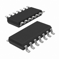
UBA2021T/N2,512 NXP Semiconductors, UBA2021T/N2,512 Datasheet - Page 6

UBA2021T/N2,512
Manufacturer Part Number
UBA2021T/N2,512
Description
IC DRIVER BALLAST CFL/TL 14SOIC
Manufacturer
NXP Semiconductors
Type
CFL/TL Driverr
Datasheet
1.UBA2021PN2112.pdf
(16 pages)
Specifications of UBA2021T/N2,512
Package / Case
14-SOIC (3.9mm Width), 14-SOL
Frequency
41.21 ~ 44.59kHz
Current - Supply
1mA
Voltage - Supply
630V
Operating Temperature
-40°C ~ 150°C
Driver Type
CFL, Fluorescent TL Drivers
Operating Supply Voltage
630 V
Maximum Operating Temperature
+ 150 C
Mounting Style
SMD/SMT
Maximum Output Current
35 mA
Maximum Power Dissipation
500 mW
Minimum Operating Temperature
- 40 C
Supply Current
1 mA
Lead Free Status / RoHS Status
Lead free / RoHS Compliant
Current - Output
-
Lead Free Status / Rohs Status
Lead free / RoHS Compliant
Other names
568-3323-5
935211250512
UBA2021T/N2
935211250512
UBA2021T/N2
Available stocks
Company
Part Number
Manufacturer
Quantity
Price
Part Number:
UBA2021T/N2,512
Manufacturer:
NXP/恩智浦
Quantity:
20 000
NXP Semiconductors
UBA2021_4
Product data sheet
7.10 IC supply
7.11 Minimum gate-source voltage of T1 and T2
7.9 Capacitive mode protection
V
purpose. This pin is also used in the preheat state and the ignition state for timing (t
t
When the preheat mode is completed, the IC will protect the power circuit against losing
the zero voltage switching condition and getting too close to the capacitive mode of
operation. This is detected by monitoring voltage V
V
Consequently the frequency increases as long as the capacitive mode is detected. The
frequency decreases down to the feed-forward frequency if no capacitive mode is
detected. Frequency modulation is achieved via the CI-pin.
Initially, the IC is supplied from V
supply capacitor CS9 via an internal diode. As soon as V
starts oscillating. After the preheat phase is finished, the pin is connected to an internal
resistor R
level at the RHV-pin thus drops from V
the VS-pin will now be charged via the snubber capacitor CS7. Excess charge is drained
by an internal clamp that turns on at voltage V
The high side driver is supplied via capacitor C
bootstrap switch during the on periods of T2. The IC stops oscillating at a voltage level
V
safeguards the minimum drive voltages V
Table 4.
The drive voltage at G2 will exceed the drive voltage of the high side driver.
FREQUENCY
< 75 kHz
75 kHz to 85 kHz
ign
Fig 6.
in
RS(cap)
VS(stop)
85 kHz
, the ripple is filtered out. The capacitor connected to the CP-pin is used for this
).
. Given a maximum charge consumption on the load at the G1-pin of 1 nC/V, this
at the time of turn-on of T2, the capacitive mode operation is assumed.
Feed-forward frequency
i(RHV)
Minimum gate-source voltages
, prior to this the RHV-pin is internally connected to the VS-pin. The voltage
(kHz)
Rev. 04 — 25 July 2008
f
frequency
bottom
in
by the current through R
VS
+ V
(G1-S1)
diode
VOLTAGE
8 V (min)
7 V (min)
6 V (min)
VS(clamp)
boot
for the high side driver, see
to I
630 V driver IC for CFL and TL lamps
. Capacitor C
RS
RHV
at the RS-pin. If the voltage is below
.
feed-forward
VS
I
RHV
R
RHV
range
exceeds V
i(RHV)
(mA)
mgs993
. This current charges the
boot
. The capacitor CS9 at
is charged via the
UBA2021
VS(start)
© NXP B.V. 2008. All rights reserved.
Table
, the circuit
1.
ph
6 of 16
and


