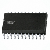
UBA2032T/N2,118 NXP Semiconductors, UBA2032T/N2,118 Datasheet - Page 6

UBA2032T/N2,118
Manufacturer Part Number
UBA2032T/N2,118
Description
IC DRIVER FULL BRIDGE SO-24
Manufacturer
NXP Semiconductors
Datasheet
1.UBA2032TSN3118.pdf
(21 pages)
Specifications of UBA2032T/N2,118
Configuration
H Bridge
Input Type
Self Oscillating
Current - Peak
130mA
Number Of Configurations
1
Number Of Outputs
4
High Side Voltage - Max (bootstrap)
550V
Voltage - Supply
10.5 V ~ 13.5 V
Operating Temperature
-40°C ~ 150°C
Mounting Type
Surface Mount
Package / Case
24-SOIC (7.5mm Width)
Lead Free Status / RoHS Status
Lead free / RoHS Compliant
Delay Time
-
Other names
935270516118
UBA2032TD-T
UBA2032TD-T
UBA2032TD-T
UBA2032TD-T
Philips Semiconductors
The oscillation can take place in three different modes:
If the supply voltage on pin V
reset level of power drive, the UBA2032 re-enters the
start-up phase. The design equation for the bridge
oscillator frequency is:
Non-overlap time
The non-overlap time is the time between turning off the
conducting pair of MOSFETs and turning on the next pair.
The non-overlap time is realized by means of an adaptive
non-overlap circuit. With an adaptive non-overlap, the
application determines the duration of the non-overlap and
makes the non-overlap time optimal for each frequency.
The non-overlap time is determined by the duration of the
falling slope of the relevant half bridge voltage (see Fig.4).
The occurrence of a slope is sensed internally. The
minimum non-overlap time is internally fixed.
2005 Mar 24
Internal oscillator mode.
In this mode the bridge commutating frequency is
determined by the values of an external resistor (R
and capacitor (C
connected to pin +LVS. To realize an accurate 50% duty
factor, the internal divider should be used. The internal
divider is enabled by connecting pin DD to pin SGND.
Due to the presence of the divider the bridge frequency
is half the oscillator frequency. The commutation of the
bridge will take place at the falling edge of the signal on
pin RC. To minimize the current consumption
pins +LVS, LVS and EXTDR can be connected
together to either pin SGND or pin V
current source in the logic voltage supply circuit is shut
off.
External oscillator mode without the internal divider.
In the external oscillator mode the external source is
connected to pin EXTDR and pin RC is short-circuited to
pin SGND to disable the internal oscillator. If the internal
divider is disabled (pin DD connected to pin V
duty factor of the bridge output signal is determined by
the external oscillator signal and the bridge frequency
equals the external oscillator frequency.
External oscillator mode with the internal divider.
The external oscillator mode can also be used with the
internal divider function enabled (pin RC and pin DD
connected to pin SGND). Due to the presence of the
divider the bridge frequency is half the external oscillator
frequency. The commutation of the bridge is triggered
by the falling edge of the EXTDR signal with respect to
V
Full bridge driver IC
LVS
.
osc
). In this mode pin EXTDR must be
f
bridge
DD
=
or pin HV drops below the
--------------------------------------------------
k
osc
DD
R
. In this way the
osc
1
C
DD
osc
) the
.
osc
)
6
Divider function
If pin DD is connected to pin SGND, then the divider
function is enabled/present. If the divider function is
present, there is no direct relation between the position of
the bridge output and the status of pin EXTDR.
Start-up delay
Normally, the circuit starts oscillating as soon as pin V
pin HV reaches the level of release power drive. At this
moment the gate drive voltage is equal to the voltage on
pin V
high side transistors. If this voltage is too low for sufficient
drive of the MOSFETs the release of the power drive can
be delayed via pin SU. A simple RC filter (R between
pin V
can be used to make a delay, or a control signal from a
processor can be used.
Bridge disable
The bridge disable function can be used to switch off all the
MOSFETs as soon as the voltage on pin BD exceeds the
bridge disable voltage (1.29 V). The bridge disable
function overrules all the other states.
handbook, halfpage
Fig.4
V half bridge right
V half bridge left
DD
DD
for the low side transistors and V
and pin SU; C between pin SU and pin SGND)
Half bridge and higher/lower side driver
output signals.
V GHR
V SHR
V GHL
V SHL
0
0
0
0
Product specification
DD
UBA2032
0.6 V for the
t (sec)
MGU545
DD
or


