ADP3110AKCPZ-RL ON Semiconductor, ADP3110AKCPZ-RL Datasheet
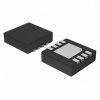
IC MOSFET DRIVER DUAL 12V 8-DFN

ADP3110AKCPZ-RL

Manufacturer Part Number
ADP3110AKCPZ-RL
Description
IC MOSFET DRIVER DUAL 12V 8-DFN
Manufacturer
ON Semiconductor
Type
High Side/Low Sider
Datasheet

Specifications of ADP3110AKCPZ-RL

Configuration
High and Low Side, Synchronous
Input Type
PWM
Delay Time
45ns
Number Of Configurations
1
Number Of Outputs
2
High Side Voltage - Max (bootstrap)
35V
Voltage - Supply
4.6 V ~ 13.2 V
Operating Temperature
0°C ~ 85°C
Mounting Type
Surface Mount
Package / Case
8-TDFN Exposed Pad
Product
MOSFET Gate Drivers
Rise Time
55 ns
Fall Time
45 ns
Propagation Delay Time
45 ns
Supply Voltage (max)
13.2 V
Supply Voltage (min)
4.15 V
Supply Current
5 mA
Maximum Operating Temperature
+ 85 C
Mounting Style
SMD/SMT
Minimum Operating Temperature
0 C
Number Of Drivers
2
Output Current
0.7 mA
Output Voltage
35 V
Lead Free Status / RoHS Status
Lead free / RoHS Compliant
Current - Peak
-
Lead Free Status / Rohs Status
Lead free / RoHS Compliant

Available stocks

Company
Part Number
Manufacturer
Quantity
Price
Part Number:
ADP3110AKCPZ-RL
Manufacturer:
ON Semiconductor
Quantity:
500
Part Number:
ADP3110AKCPZ-RL
Manufacturer:
ON/安森美
Quantity:
20 000
Company:
Part Number:
ADP3110AKCPZ-RL
Quantity:
200
ADP3110A
Dual Bootstrapped, 12 V
MOSFET Driver with Output
Disable
optimized to drive the gates of both high−side and low−side power
MOSFETs in a synchronous buck converter. The high−side and
low−side driver is capable of driving a 3000 pF load with a 25 ns
propagation delay and a 30 ns transition time.
gate drive voltage can be optimized for the best efficiency. Internal
adaptive nonoverlap circuitry further reduces switching losses by
preventing simultaneous conduction of both MOSFETs.
high as 35 V, with transient voltages as high as 40 V. Both gate outputs
can be driven low by applying a low logic level to the Output Disable
(OD) pin. An Undervoltage Lockout function ensures that both driver
outputs are low when the supply voltage is low, and a Thermal
Shutdown function provides the IC with overtemperature protection.
Features
Applications
© Semiconductor Components Industries, LLC, 2008
August, 2008 − Rev. 4
The ADP3110A is a single Phase 12 V MOSFET gate drivers
With a wide operating voltage range, high or low side MOSFET
The floating top driver design can accommodate VBST voltages as
when Used with Patented FlexModet Controller
All−In−One Synchronous Buck Driver
Bootstrapped High−Side Drive
One PWM Signal Generates Both Drives
Anticross Conduction Protection Circuitry
OD for Disabling the Driver Outputs Meets CPU VR Requirement
These are Pb−Free Devices
Multiphase Desktop CPU Supplies
Single−Supply Synchronous Buck Converters
1
ADP3110AKRZ
ADP3110AKRZ−RL
ADP3110AKCPZ−RL
†For information on tape and reel specifications,
including part orientation and tape sizes, please
refer to our Tape and Reel Packaging Specification
Brochure, BRD8011/D.
8
Device
1
1
ORDERING INFORMATION
BST
V
OD
BST
V
CC
IN
OD
A = Assembly Location
L = Wafer Lot
Y = Year
W = Work Week
G = Pb−Free Package
CC
PIN CONNECTIONS
IN
http://onsemi.com
1
CASE 506BJ
1
MN SUFFIX
CASE 751
D SUFFIX
(Top View)
DFN8
SO−8
(Pb−Free)
(Pb−Free)
(Pb−Free)
Package
DFN8
SO−8
SO−8
Publication Order Number:
8
8
2500 Tape & Reel
5000 Tape & Reel
DRVH
SWN
PGND
DRVL
1
98 Units / Rail
DIAGRAMS
DRVH
SWN
PGND
DRVL
8
1
Shipping
MARKING
ADP3110A/D
ALYWG
3110A
ALYW
L3E
G
G
8

Related parts for ADP3110AKCPZ-RL

ADP3110AKCPZ-RL Summary of contents

Page 1

... View) ORDERING INFORMATION Device Package ADP3110AKRZ SO−8 (Pb−Free) ADP3110AKRZ−RL SO−8 (Pb−Free) ADP3110AKCPZ−RL DFN8 (Pb−Free) †For information on tape and reel specifications, including part orientation and tape sizes, please refer to our Tape and Reel Packaging Specification Brochure, BRD8011/D. 1 MARKING DIAGRAMS ...

Page 2

OD V TSD CC UVLO 2 IN START STOP MIN DRVL OFF TIMER PIN DESCRIPTION SO−8 DFN8 Symbol 1 1 BST Upper MOSFET Floating Bootstrap Supply. A capacitor connected between BST and SW pins holds this bootstrap voltage for ...

Page 3

MAXIMUM RATINGS Operating Ambient Temperature Operating Junction Temperature, T (Note 1) J Package Thermal Resistance: SO−8 Junction−to−Case, R qJC Junction−to−Ambient, R (2−Layer Board) qJA Package Thermal Resistance: DFN8 (Note 2) Junction−to−Case, R (From die to exposed pad) qJC ...

Page 4

ELECTRICAL CHARACTERISTICS Characteristic Supply Supply Voltage Range Supply Current OD Input Input Voltage High Input Voltage Low Hysteresis Input Current PWM Input Input Voltage High Input Voltage Low Hysteresis Input Current High−Side Driver Output Resistance, Sourcing Current Output Resistance, Sinking ...

Page 5

Theory of Operation The ADP3110A are single phase MOSFET drivers designed for driving two N−channel MOSFETs in a synchronous buck converter topology. The ADP3110A will operate from 5 but have been optimized for high current multi−phase ...

Page 6

OD V OD_LO DRVH or DRVL Figure 2. Output Disable Timing Diagram V PWM_HI pdlDRVL fDRVL 90% DRVL 2V DRVH−SW SW Figure 3. Nonoverlap Timing Diagram Output Enable 2 PWM in Figure 4. ...

Page 7

... 0.10 0.05 BOTTOM VIEW *For additional information on our Pb−Free strategy and soldering details, please download the ON Semiconductor Soldering and Mounting Techniques Reference Manual, SOLDERRM/D. PACKAGE DIMENSIONS DFN8 3x3, 0.5P CASE 506BJ−01 ISSUE O EDGE OF PACKAGE L L1 DETAIL A OPTIONAL CONSTRUCTION L DETAIL A OPTIONAL ...

Page 8

... *For additional information on our Pb−Free strategy and soldering details, please download the ON Semiconductor Soldering and Mounting Techniques Reference Manual, SOLDERRM/D. FlexMode is a trademark of Analog Devices, Inc. ON Semiconductor and are registered trademarks of Semiconductor Components Industries, LLC (SCILLC). SCILLC reserves the right to make changes without further notice to any products herein ...

Related keywords