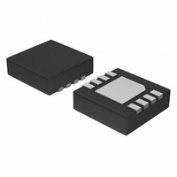
ADP3110AKCPZ-RL ON Semiconductor, ADP3110AKCPZ-RL Datasheet - Page 4

ADP3110AKCPZ-RL
Manufacturer Part Number
ADP3110AKCPZ-RL
Description
IC MOSFET DRIVER DUAL 12V 8-DFN
Manufacturer
ON Semiconductor
Type
High Side/Low Sider
Datasheet
1.ADP3110AKCPZ-RL.pdf
(8 pages)
Specifications of ADP3110AKCPZ-RL
Configuration
High and Low Side, Synchronous
Input Type
PWM
Delay Time
45ns
Number Of Configurations
1
Number Of Outputs
2
High Side Voltage - Max (bootstrap)
35V
Voltage - Supply
4.6 V ~ 13.2 V
Operating Temperature
0°C ~ 85°C
Mounting Type
Surface Mount
Package / Case
8-TDFN Exposed Pad
Product
MOSFET Gate Drivers
Rise Time
55 ns
Fall Time
45 ns
Propagation Delay Time
45 ns
Supply Voltage (max)
13.2 V
Supply Voltage (min)
4.15 V
Supply Current
5 mA
Maximum Operating Temperature
+ 85 C
Mounting Style
SMD/SMT
Minimum Operating Temperature
0 C
Number Of Drivers
2
Output Current
0.7 mA
Output Voltage
35 V
Lead Free Status / RoHS Status
Lead free / RoHS Compliant
Current - Peak
-
Lead Free Status / Rohs Status
Lead free / RoHS Compliant
Available stocks
Company
Part Number
Manufacturer
Quantity
Price
Company:
Part Number:
ADP3110AKCPZ-RL
Manufacturer:
ON Semiconductor
Quantity:
500
Part Number:
ADP3110AKCPZ-RL
Manufacturer:
ON/安森美
Quantity:
20 000
4. All limits at temperature extremes are guaranteed via correlation using standard Statistical Quality Control (SQC).
5. For propagation delays, “tpdh” refers to the specified signal going high; “tpdl” refers to it going low.
6. Guaranteed by design; not tested in production.
ELECTRICAL CHARACTERISTICS
Supply
OD Input
PWM Input
High−Side Driver
Low−Side Driver
Undervoltage Lockout
Supply Voltage Range
Supply Current
Input Voltage High
Input Voltage Low
Hysteresis
Input Current
Input Voltage High
Input Voltage Low
Hysteresis
Input Current
Output Resistance, Sourcing Current
Output Resistance, Sinking Current
Output Resistance, Unbiased
Transition Times
Propagation Delay Times (Note 5)
SW Pulldown Resitance
Output Resistance, Sourcing Current
Output Resistance, Sinking Current
Output Resistance, Unbiased
Transition Times
Propagation Delay Times (Note 5)
Timeout Delay
UVLO Startup
UVLO Shutdown
Hysteresis
Characteristic
(Note 4) (V
V
V
t
t
Symbol
t
V
t
pdhDRVH
V
pdhDRVL
pdlDRVH
PWM_LO
t
t
pdlDRVL
t
t
t
PWM_HI
t
t
t
rDRVH
fDRVH
pdhOD
pdhOD
OD_LO
rDRVL
fDRVL
pdlOD
pdlOD
V
I
OD_HI
SYS
CC
−
−
−
−
−
−
−
−
−
−
−
−
−
CC
= 12 V, T
No internal pullup or pulldown resistors
No internal pullup or pulldown resistors
http://onsemi.com
BST − SW = 12 V, C
BST − SW = 12 V, C
BST − SW = 12 V, C
C
C
LOAD
LOAD
A
(Note 6, t
BST = 12 V, IN = 0 V
= 0°C to +85°C, T
BST − SW = 12 V
BST − SW = 12 V
BST − SW = 0 V
= 3.0 nF, (See Figure 3)
= 3.0 nF, (See Figure 3)
DRVH − SW = 0
4
(See Figure 3)
(See Figure 3)
(See Figure 2)
(See Figure 2)
(See Figure 2)
(See Figure 2)
SW to PGND
V
Condition
CC
pdhDRVL
= PGND
−
−
−
−
−
−
−
−
−
−
LOAD
LOAD
LOAD
only)
J
= 3.0 nF
= 3.0 nF
= 3.0 nF
= 0°C to +125°C unless otherwise noted.)
−1.0
−1.0
Min
4.6
2.0
2.0
3.9
3.7
0.1
32
−
−
−
−
−
−
−
−
−
−
−
−
−
−
−
−
Typ
400
400
0.7
2.2
1.0
1.8
1.0
4.3
4.1
0.2
15
20
45
25
20
25
15
15
16
12
15
20
20
85
11
11
−
−
−
−
−
−
−
Max
13.2
+1.0
+1.0
5.0
0.8
0.8
3.4
1.8
3.4
1.8
4.5
4.3
0.4
55
45
70
35
35
55
50
30
35
40
35
35
−
−
−
−
−
−
−
−
Unit
mA
mV
mV
kW
kW
kW
mA
mA
ns
ns
ns
ns
ns
W
W
W
W
V
V
V
V
V
V
V
V


